Maybe I’m just expecting too much from enterprise.
1 Like
Haha.
Enterprise gets a bad rap for a lot of stuff, but it comes down to dollars and cents.
As i said we’re pretty helpless to fix the software, moving off of it will cost > $1m (and is considered a large commercial risk) and it currently “does the job”. Better the devil you know, etc. That $1m isn’t even including re-training the few hundred or so users of this application that we have.
Everybody hates the program, but we know its quirks and how to make it work.
Trying to convince those who control the purse strings that you want to ditch an application like that, for that sort of money with significant commercial risk is extremely difficult. :-\
And at the end of the day you can totally see why from their perspective. What do they get for their money? A bunch of intangibles that are impossible to demonstrate prior to actually changing…
1 Like
And I absolutely don’t blame them for it. I’m a software idealist, so I get lost in my own hopes and dreams sometimes.
1 Like
Actually i just had a thought…
Applications like this don’t make use of things like:
- AES
- MMX, 3dnow, AVX
- huge core count
- crypto
- graphics
- etc.
Would be interesting to see what intel or AMD or whoever could do with a large die that focused purely on running dumb old x86/x64 code as fast as possible. No special instruction set extensions. Just focus on giving whatever space is required between components for heat dissipation (e.g., dark silicon like Ryzen 12nm), enough pipeline stages for high clock, massive cache, etc.
Like a modern day P4 netburst on steroids…
Then again, i guess keeping the modern instruction set extensions is probably “cheap” (silicon wise) in the context of adding massive amounts of cache…
Interesting thought…
I don’t really know enough, so it’s hard to speculate…
x86 is really messy instruction set wise because its nothing but patches upon patches since intels first cpu. This also means that there is ALOT of complexity. Reducing complexity means that compatibility with become less and less. You will eventually get to a point where just making a whole new instruction set would be a serious consideration.
I think you misunderstand my point. I’m not saying to simplify x86 or x64. I’m saying to build a processor that just runs the base level of x64 instructions from say 2001.
The instructions that most enterprise apps built 10-20 or more years ago would use.
I really don’t want to derail this thread into architecture but x86 is really messed up. This guy got root access on a VIA platform over a RISC embedded processor. Granted it’s only one platform but still.
Intel and co should put more manpower into cutting out bullshit instructions like that.
First three minutes after that it’s the explanation.
That was really good, still watching it. Thanks.
@thro do you thin that turbo x86 was what Intel was thinking about back in P4 days when they said 10ghz CPUs were the future.
Side note, people just need this so that’s way I am posting it here. NewPipe’s ability to overlay a video wand let you keep using the app underneath is amazing. I was watching the video while drilling through this and reading and replying as I am doing now, just moving the video out of my way to get at buttons I need. You can even shrink the video into a corner. I just like having it across the screen.

1 Like
Definitely, and glad to see someone else here remembers. IIRC intel were predicting 10 Ghz by say 2005 or something? If you’d been looking at history as an indicator of future trends, that would be about right, too.
Well. I don’t think they were deliberately trying to strip x86 down to dumb x86 code, there were still extensions added with the P4.
But the P4 was most definitely a bet on frequency scaling that did not pan out.
The P4 was built to scale to 10Ghz on silicon. That’s why its pipelines were so long, why it was initially configured for RAMBUS RDRAM, etc.
The design for its intended environment was probably sound.
Unfortunately for intel, silicon hit a wall around 3-4 Ghz and those clocks simply aren’t quick enough for the P4 design to really shine. At the slow clocks it ended up running at vs. what it was intended for, it sucked.
It is very much worth remembering that we hit 3 Ghz back in 2002!
Back in 2000, 1.0 Ghz was bleeding edge, and only a couple of years prior the Pentium 3 450mhz was top dog!
Clock rate was literally doubling every couple of years until 2002, and since then increase in clock has been very very slow.
1 Like
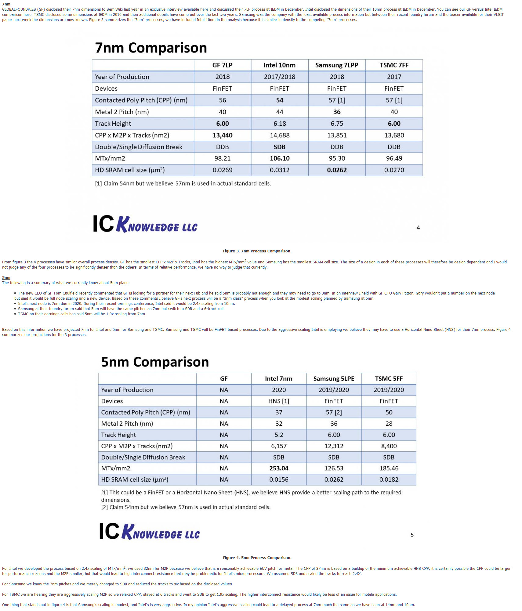
Update from Samsung.
7nm EUV set for high volume manufacturing in 2019.
Plans to use GAAFETs on their 3nm node.
5/4nm node planned for risk production in 2019.
https://www.anandtech.com/show/13329/samsung-foundry-updates-8lpu-for-2019
1 Like
The last guy that asks a question sounds allot like Joe Scott! Must say this video was very informative! Thanks for linking!
1 Like
Still wondering if we’ll ever see gallium arsenide CPUs for consumer…
1 Like
So, first post. This is coming from a discussion on another forum, so if I do not scrub my tone from there, please ignore it. This is to give a lot of information about the process density and recent industry happenings.
Here is what I am talking about:
https://www.eetimes.com/document.asp?doc_id=1333657
And this, which is densiity calculations before Intel making their node less dense was announced at the end of July to the beginning of Aug. This is from June 25, 2018
Now, the fact Intel is ceding EUV lead to samsung and TSMC shows that the statements hedging to benefit Intel in the WCCFTech article will not occur. Then you have Apple and Qualcomm rejecting Intel’s radios, causing Intel scrapping their 5G modem plans after both rejected Intel. Also, months ago, Apple suggested that they may develop a CPU in house (likely meaning laptop and desktop, possibly on ARM at 7nm and below).
Then you have ARM attacking Intel’s i5-U series (https://appuals.com/arm-roadmap-2018-20-intel/):
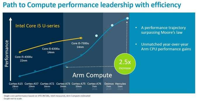
And you have Intel saying they are trying to hold AMD to 15% market share next year in servers:
https://www.tomshardware.com/news/intel-ceo-amd-server-market,37273.html
Intel’s former CEO while he was CEO in June said it is Intel’s goal to hold AMD to 15-20% market share for servers next year.
https://www.extremetech.com/computing/276376-intel-reportedly-wont-deploy-euv-lithography-until-2021
And if you didn’t hear, AMD is fabbing ALL 7nm designs with TSMC and GF is abandoning their 7nm node and future node shrinks for the moment. But, GF and Intel may be working on 12nm FD-SOI together. The roadmap image was removed. But, either way, 12nm FD-SOI, likely taping out next year, uses .40V and is considered to be the equivalent of an industry 10nm (not talking Intel’s, whose 10nm is the same, roughly, as other fabs 7nm). (currently reading articles on this at the moment). This was a recent pivot decision by the new CEO to focus on financial success rather than trying to be at the cutting edge.
Here is what is going on with Samsung: https://www.anandtech.com/show/13329/samsung-foundry-updates-8lpu-for-2019
1 Like
I also brought this up in the thread about Global Foundries dropping 7 nm
Does anyone have any thoughts about what will happen with IBM’s chip production?
Currently they have a custom SOI 14 nm node at Global Foundries that is used for their POWER9 and z14 chips. POWER10 is planned for 2020, and I assume z15 is probably also in development, so where would IBM be making these chips?
The IBM/GF agreement made GF the sole chip manufacturer for IBM until at least 2024, will that be renegotiated? Would IBM do something as dramatic as buying back the fabs in Essex Junction and East Fishkill (GF Fabs 9 and 10)? It looks like IBM still does process research for new nodes, so maybe this isn’t as far fetched as I think?
GF, IBM, and Samsung used to work together through the Common Platform alliance; while that’s gone, there is still the IBM Research Alliance between the three companies. With that in place, Samsung would therefore be the candidate for POWER10/z15 manufacturing, right?
Also, with IBM’s chips being used in US government Supercomputers, is there a requirement for chips to be domestically manufactured?
Edit: found this quote from an IBM executive in a NextPlatform article:
Our agreement with GlobalFoundries was not into perpetuity for all technology nodes, It was focused on 22 nanometers and then 14 nanometers and one more node – not a couple of nodes – beyond that. We were evaluating the field anyway.
and the article does a lot of the same speculation I was asking about above. Still, I would be interested what you think about all this.
1 Like
So, considering IBM stated only one more node, it is likely discussing 12FDX hybrid, similar to the 14nm hybrid they are doing utilizing finFET with SOI.
https://www.globalfoundries.com/technology-solutions/cmos/fdx/12fdx
http://soiconsortium.eu/wp-content/uploads/2017/08/FDSOI-Technology-Overview_BY-Nguyen_Nanjing-Sept-22-2017_Final.pdf (page 32 shows 12/10nm as the next step from the 14nm node)
http://www.semi.org/eu/sites/semi.org/files/events/presentations/03_Gerd%20Teepe_GLOBALFOUNDRIES.pdf
https://www.semiwiki.com/forum/content/6248-glofos-12nm-fd-soi-why-makes-headlines-china.html
Now, FD-SOI is closer to planar transistors for many uses, but there is no reason finfet and SOI must be exclusive. This is what IBM’s process is about. Then, at 3nm, the GAA usually discusses either using nanowires or nanosheets. When done in a horizontal orientation, the nanosheets will have similar issues on uniformity that were had before finFET, but there are similarities to SOI for nanosheets, so it isn’t fully a loss there.
Now, Intel has named one of their upcoming architectures Sapphire Rapids. One of the types of SOI is SOS, which is silicon on sapphire. This may suggest Intel is considering using a nanosheet design with SOI with the insulator being sapphire.
But that is moving away from your ask. Unless GF, which is doing an ASIC subsidiary which plans to license 7nm, has the ASIC capacity to slightly modify it to allow IBM processors to be made on an ASIC line (doubtful), I’m going with the 12FDX with extremely low energy requirements for the node below 14nm, then allowing IBM the freedom of either Samsung or TSMC, but, as you mentioned, there may be reasons to suspect Samsung as more likely. But, that’s my thoughts on it.
1 Like
This has to hurt chipzillas pride.
Moving some chipset production to TSMC
https://techreport.com/news/34078/report-intel-could-move-some-chipset-production-to-tsmc
3 Likes
Interesting; which TSMC node size would be most equivalent to Intel’s 14nm though?
If Intel-14nm is closer to TSMC-12nm than TSMC-7nm, maybe GlobalFoundries’ 12FDX as mentioned by @ajc9988 would also be a candidate?
That’s an interesting thought, who would have more spare fab capacity?
TSMC is larger than GF AFAIK, but with Apple, Nvidia, and AMD all using TSMC’s leading nodes, do they really have that much spare capacity either?
I would definitely assume TSMCs 12nm or 10nm node.
1 Like
I very much suspect that Samsung and TSMC are going to overtake intel eventually in terms of fab, if not already at 7nm, definitely shortly thereafter. The iPad Pro CPU is an example of just what these guys can put out in extremely low power consumption… whether you like apple or not there is no denying that the chip in this device (and most likely the android phones, etc. as well) is amazingly impressive.
They’re generally making the bulk of the small dies for things like phones, tablets, IoT devices, etc. and the sheer economy of scale they can get will be way better than intel. Intel has tried to diversify into mobile and failed. X86 plus Windows is no longer the lever it used to be in the 90s.
Whilst intel might knock out a few hundred million CPUs or whatever, Samsung and TSMC are shipping way, way more than that and the bulk of their dies are small so their yields can be better even with the same defect density. i.e., they can lead with a smaller product until the process is refined. Intels dies are generally large, compared to say an ARM SOC. On the flip-side, TSMC and Samsung are likely getting the third party GPU manufacturing from AMD and Nvidia for the foreseeable future, so they also have scope for larger dies to make bank on, once the process is mature.
I believe that the days of intel being unassailable due to their fab advantage are OVER. In order to fund new fabs, like anyone else, they need to ship products to make money to fund them, and the x86 CPU market is less important now.
The bulk of the money is shifting to ARM based products and GPUs and intel are a total no-show in both of those markets. Optane is also a “meh” niche product - samsung are killing them in solid state storage as well. Fact is, intel haven’t had a killer product outside of x86 for a very long time now. If ever?
AMD switching to TSMC for their production is going to be very, very interesting indeed. I firmly believe that they’ve been held back significantly by Global Foundries contractual obligations, and look forward to seeing what their CPU and GPU designs can do once their performance potential is realised via TSMC.
edit:
put it this way: if intel fabs were so amazingly great, surely Nvidia would look into some sort of agreement with intel to get capacity on said fabs? License some Nvidia IP to intel (which surely intel would be desperate for) in return for it to kill AMD via exclusive fab superiority? I don’t believe they’ve even tried that?