The Bleeding Edge [Semiconductor Foundry Thread]

Definitely, and glad to see someone else here remembers. IIRC intel were predicting 10 Ghz by say 2005 or something? If you’d been looking at history as an indicator of future trends, that would be about right, too.

Well. I don’t think they were deliberately trying to strip x86 down to dumb x86 code, there were still extensions added with the P4.

But the P4 was most definitely a bet on frequency scaling that did not pan out.

The P4 was built to scale to 10Ghz on silicon. That’s why its pipelines were so long, why it was initially configured for RAMBUS RDRAM, etc.

The design for its intended environment was probably sound.

Unfortunately for intel, silicon hit a wall around 3-4 Ghz and those clocks simply aren’t quick enough for the P4 design to really shine. At the slow clocks it ended up running at vs. what it was intended for, it sucked.

It is very much worth remembering that we hit 3 Ghz back in 2002!

Back in 2000, 1.0 Ghz was bleeding edge, and only a couple of years prior the Pentium 3 450mhz was top dog!

Clock rate was literally doubling every couple of years until 2002, and since then increase in clock has been very very slow.

1 Like

Update from Samsung.
7nm EUV set for high volume manufacturing in 2019.
Plans to use GAAFETs on their 3nm node.
5/4nm node planned for risk production in 2019.

https://www.anandtech.com/show/13329/samsung-foundry-updates-8lpu-for-2019

1 Like

The last guy that asks a question sounds allot like Joe Scott! Must say this video was very informative! Thanks for linking!

1 Like

Still wondering if we’ll ever see gallium arsenide CPUs for consumer…

1 Like

So, first post. This is coming from a discussion on another forum, so if I do not scrub my tone from there, please ignore it. This is to give a lot of information about the process density and recent industry happenings.

Here is what I am talking about:
https://www.eetimes.com/document.asp?doc_id=1333657

And this, which is densiity calculations before Intel making their node less dense was announced at the end of July to the beginning of Aug. This is from June 25, 2018

[Chart from semiwiki]


Now, the fact Intel is ceding EUV lead to samsung and TSMC shows that the statements hedging to benefit Intel in the WCCFTech article will not occur. Then you have Apple and Qualcomm rejecting Intel’s radios, causing Intel scrapping their 5G modem plans after both rejected Intel. Also, months ago, Apple suggested that they may develop a CPU in house (likely meaning laptop and desktop, possibly on ARM at 7nm and below).

Then you have ARM attacking Intel’s i5-U series (https://appuals.com/arm-roadmap-2018-20-intel/):
image
And you have Intel saying they are trying to hold AMD to 15% market share next year in servers:
https://www.tomshardware.com/news/intel-ceo-amd-server-market,37273.html
Intel’s former CEO while he was CEO in June said it is Intel’s goal to hold AMD to 15-20% market share for servers next year.
https://www.extremetech.com/computing/276376-intel-reportedly-wont-deploy-euv-lithography-until-2021

And if you didn’t hear, AMD is fabbing ALL 7nm designs with TSMC and GF is abandoning their 7nm node and future node shrinks for the moment. But, GF and Intel may be working on 12nm FD-SOI together. The roadmap image was removed. But, either way, 12nm FD-SOI, likely taping out next year, uses .40V and is considered to be the equivalent of an industry 10nm (not talking Intel’s, whose 10nm is the same, roughly, as other fabs 7nm). (currently reading articles on this at the moment). This was a recent pivot decision by the new CEO to focus on financial success rather than trying to be at the cutting edge.

Here is what is going on with Samsung: https://www.anandtech.com/show/13329/samsung-foundry-updates-8lpu-for-2019

1 Like

I also brought this up in the thread about Global Foundries dropping 7 nm

Does anyone have any thoughts about what will happen with IBM’s chip production?
Currently they have a custom SOI 14 nm node at Global Foundries that is used for their POWER9 and z14 chips. POWER10 is planned for 2020, and I assume z15 is probably also in development, so where would IBM be making these chips?

The IBM/GF agreement made GF the sole chip manufacturer for IBM until at least 2024, will that be renegotiated? Would IBM do something as dramatic as buying back the fabs in Essex Junction and East Fishkill (GF Fabs 9 and 10)? It looks like IBM still does process research for new nodes, so maybe this isn’t as far fetched as I think?

GF, IBM, and Samsung used to work together through the Common Platform alliance; while that’s gone, there is still the IBM Research Alliance between the three companies. With that in place, Samsung would therefore be the candidate for POWER10/z15 manufacturing, right?

Also, with IBM’s chips being used in US government Supercomputers, is there a requirement for chips to be domestically manufactured?


Edit: found this quote from an IBM executive in a NextPlatform article:

Our agreement with GlobalFoundries was not into perpetuity for all technology nodes, It was focused on 22 nanometers and then 14 nanometers and one more node – not a couple of nodes – beyond that. We were evaluating the field anyway.

and the article does a lot of the same speculation I was asking about above. Still, I would be interested what you think about all this.

1 Like

So, considering IBM stated only one more node, it is likely discussing 12FDX hybrid, similar to the 14nm hybrid they are doing utilizing finFET with SOI.

https://www.globalfoundries.com/technology-solutions/cmos/fdx/12fdx
http://soiconsortium.eu/wp-content/uploads/2017/08/FDSOI-Technology-Overview_BY-Nguyen_Nanjing-Sept-22-2017_Final.pdf (page 32 shows 12/10nm as the next step from the 14nm node)
http://www.semi.org/eu/sites/semi.org/files/events/presentations/03_Gerd%20Teepe_GLOBALFOUNDRIES.pdf
https://www.semiwiki.com/forum/content/6248-glofos-12nm-fd-soi-why-makes-headlines-china.html

Now, FD-SOI is closer to planar transistors for many uses, but there is no reason finfet and SOI must be exclusive. This is what IBM’s process is about. Then, at 3nm, the GAA usually discusses either using nanowires or nanosheets. When done in a horizontal orientation, the nanosheets will have similar issues on uniformity that were had before finFET, but there are similarities to SOI for nanosheets, so it isn’t fully a loss there.

Now, Intel has named one of their upcoming architectures Sapphire Rapids. One of the types of SOI is SOS, which is silicon on sapphire. This may suggest Intel is considering using a nanosheet design with SOI with the insulator being sapphire.

But that is moving away from your ask. Unless GF, which is doing an ASIC subsidiary which plans to license 7nm, has the ASIC capacity to slightly modify it to allow IBM processors to be made on an ASIC line (doubtful), I’m going with the 12FDX with extremely low energy requirements for the node below 14nm, then allowing IBM the freedom of either Samsung or TSMC, but, as you mentioned, there may be reasons to suspect Samsung as more likely. But, that’s my thoughts on it.

1 Like

This has to hurt chipzillas pride.

Moving some chipset production to TSMC

https://techreport.com/news/34078/report-intel-could-move-some-chipset-production-to-tsmc

3 Likes

Interesting; which TSMC node size would be most equivalent to Intel’s 14nm though?

If Intel-14nm is closer to TSMC-12nm than TSMC-7nm, maybe GlobalFoundries’ 12FDX as mentioned by @ajc9988 would also be a candidate?

That’s an interesting thought, who would have more spare fab capacity?
TSMC is larger than GF AFAIK, but with Apple, Nvidia, and AMD all using TSMC’s leading nodes, do they really have that much spare capacity either?

I would definitely assume TSMCs 12nm or 10nm node.

1 Like

I very much suspect that Samsung and TSMC are going to overtake intel eventually in terms of fab, if not already at 7nm, definitely shortly thereafter. The iPad Pro CPU is an example of just what these guys can put out in extremely low power consumption… whether you like apple or not there is no denying that the chip in this device (and most likely the android phones, etc. as well) is amazingly impressive.

They’re generally making the bulk of the small dies for things like phones, tablets, IoT devices, etc. and the sheer economy of scale they can get will be way better than intel. Intel has tried to diversify into mobile and failed. X86 plus Windows is no longer the lever it used to be in the 90s.

Whilst intel might knock out a few hundred million CPUs or whatever, Samsung and TSMC are shipping way, way more than that and the bulk of their dies are small so their yields can be better even with the same defect density. i.e., they can lead with a smaller product until the process is refined. Intels dies are generally large, compared to say an ARM SOC. On the flip-side, TSMC and Samsung are likely getting the third party GPU manufacturing from AMD and Nvidia for the foreseeable future, so they also have scope for larger dies to make bank on, once the process is mature.

I believe that the days of intel being unassailable due to their fab advantage are OVER. In order to fund new fabs, like anyone else, they need to ship products to make money to fund them, and the x86 CPU market is less important now.

The bulk of the money is shifting to ARM based products and GPUs and intel are a total no-show in both of those markets. Optane is also a “meh” niche product - samsung are killing them in solid state storage as well. Fact is, intel haven’t had a killer product outside of x86 for a very long time now. If ever?

AMD switching to TSMC for their production is going to be very, very interesting indeed. I firmly believe that they’ve been held back significantly by Global Foundries contractual obligations, and look forward to seeing what their CPU and GPU designs can do once their performance potential is realised via TSMC.

edit:
put it this way: if intel fabs were so amazingly great, surely Nvidia would look into some sort of agreement with intel to get capacity on said fabs? License some Nvidia IP to intel (which surely intel would be desperate for) in return for it to kill AMD via exclusive fab superiority? I don’t believe they’ve even tried that?

So, first is to understand that TSMC 12nm is actually a refined 16nm process. It would be like Intel’s 14nm+ (not saying they are equivalent here, rather saying they are iterations from the first generation process).
http://www.tsmc.com/english/dedicatedFoundry/technology/16nm.htm


So, you would either be looking at TSMC 12nm half node-ish type refinement (I don’t know it is a full half-node as defined in certain ways, but some articles, nonetheless, have presented it as such) versus a large process refinement, or the 10FF design, which likely compares well and may be slightly more dense than Intel’s 14nm, or is at least comparable. I haven’t looked at the hard numbers to see whether the density compares best for 10FF against Intel’s 14nm, 14nm+, or 14nm++, so I am not speaking to that, and yes, Intel’s refined 14nm processes may be denser than 10FF, I just haven’t looked at the numbers and could not find something this morning to give hard numbers. I may revisit this at the end of the day to give a firm answer. But, that should give a bit better idea that if they used a process from TSMC, the 10FF would be the closest, but that makes up very little of TSMC’s current production. Intel could do 12FF, but that is very close to the 16FF+, so may or may not be an answer (although it is better than 22nm).

Now, 12FDX is closer to industry 10nm designs according to what I have read, and Samsung and TSMC 10nm is closer to around Intel 14nm. I’m not sure when volume 12nm FD-SOI will be available from GF, though, and it may be closer to 2020, which may rule out GF 12FDX from consideration, leaving only the 12nm finFET design, which might not be a great fit for Intel.

But very interesting overall…

Edit: @wendell - Just got done watching the L1T news and noticed you mentioned III-V materials for Intel’s 10nm. I wanted to provide some more resources for you, as I believe those come into play more at 7nm and below for Intel, and smaller than 7nm for other fabs, which include nanowire and nanosheet use in Gate All Around implementations. I have some links above already, but here are some more relevant to the discussion:

https://fuse.wikichip.org/news/525/iedm-2017-isscc-2018-intels-10nm-switching-to-cobalt-interconnects/
IEDM conference website: https://ieee-iedm.org/ (Dec. 1-5, 2018)


https://www.eetimes.com/document.asp?doc_id=1332328


Forum discussion on Intel 10nm and density.

Node trends and calculations from last year:


Great read for transistors and density comparison from last December of Intel 10nm and GF 7nm (now defunct)

Even though no longer being used, for those that want a bit deeper dive on GF7nm and cobalt discussion, here is IEDM of GF 7nm

Here is an article from March 29, 2017 for the press day in which Intel said 10nm would have 25% performance and 45% better power efficiency, but this was long before they gutted 10nm (see the articles I posted above for the “12nm” stuff, or review the articles from semiaccurate on the topic), which could mean less transistor density than the 2.7X promised, which means that the performance and power efficiency numbers also would be incorrect.


Intel’s own projections have both 10nm and 10nm+ performing lower than 14nm++. If this is still correct, and considering the gutting to get 10nm out the door, it should be and could be even more of a gap than from 2017, we see a situation where Intel may be pushing all 14nm++ due to not getting 10nm out due to issues in quad patterning and transistor defects, which would be amplified due to having a single dummy gate, which if the defects showed up in the dummy gates, you no longer have two dummy gates to guarantee the transistors work, which could drastically effect yields, etc. This is why, in my belief, Intel did not want to create Cascade or Cooper on 14nm++, which could cannibalize sales of Ice Lake-SP/AP in 2020 as not really offering as much of a jump. This is before talking about tiger lake or granite rapids, etc., which then look to be 2021 and beyond.

Hope this additional information is well received.

3 Likes

So the impression I’m getting is that in terms of volume:

TSMC > Samsung > Intel > GlobalFoundries

The thing I don’t get is why GF was so low in the pile? My understanding for the reason GF was divested/spun-off/whatever from AMD was that they had built too many fabs. So, we have:

too-many AMD fabs + IBM fabs + newly built fabs = not enough capacity

What gives? And they even had Abu Dhabi funding and a talent pool from AMD+IBM to start off from. How did GF manage to torpedo themselves out of 7nm competition with a deck that looks stacked in their favor?

Or maybe put a different way, how do Samsung and TSMC survive when GF cannot?

  • GF has guaranteed customers in AMD and IBM
  • Samsung has its own products to drive volume
  • TSMC has ?

TSMC has Nvidia, but they are more than willing to jump ship if needed.


Sorry if I’m monopolizing the thread talking about GF, who is no longer technically bleeding edge anymore, but it makes absolutely no sense to me why they couldn’t succeed.

Does TSMC make most of their money from many smaller customers? If so, why couldn’t GF serve the same market?


Maybe a good question in general, how much do non-leading-edge nodes subsidize bleeding edge development for these sorts of companies? Are their any charts showing what percentage of output from different companies is different node sizes?

1 Like

The answer is simple - cost.


When we are talking about the cost to design at 7nm, including getting the masks correct (which masks and pellicles is an issue for EUV, but decreases the quad patterning), it costs a lot more to play on that node. There was a larger expectation that ASIC designers and low power chip designers would pick up 7nm quickly, but with Nvidia seemingly waiting for 7nm EUV, as it seems some others are doing, we have Qualcomm Snapdragon, a Samsung 7nm ARM chip, Apple’s recent chip (fabbed by TSMC), and AMD’s designs that are for sure 7nm this year and 1H 2019. That, in the modern world of IoT and mobile devices, really isn’t a lot. So, GF likely didn’t have enough interest in their 7nm to make it commercially viable, especially with some reports suggesting it would have taken another $2B in expenses to get their 7nm off the ground.

So, they took the time to pivot, by focusing on low power solutions, spinning off an ASIC subsidiary that can license 7nm as needed (likely reducing the cost of 7nm implementation), etc.

Now, when IBM paid GF to take their fab and keep on their fab employees for years, that made GF a larger foundry than Intel. This decision of a pivot came from the new CEO appointed this past spring. Considering IBM only has one more node of being locked in, there is a chance that GF couldn’t get IBM to dance, just like they missed the chance to dance with their old sweetie AMD. So focusing on 12 FDX is a way to look for the markets that are not moving to 7nm with Samsung and TSMC in the next year or two and saying, hey, we have this process that isn’t as good as 7nm, but it does the job and you don’t have to worry as much on yields, development, etc. I can see how that makes a certain level of sense, especially since 10nm is still a strong performing node, but it also comes with 0.4-0.5V, which is lower power solutions than you would get otherwise. It was a decision of instead of trying to compete with the body builders TSMC and Samsung to instead go to another bar and try picking up women over there, without having to constantly try flexing to keep up with the other two. They offer lower cost for development, low energy requirements, and plenty of fab capacity to deal with what may come.

And, there is an interesting examination of the consolidation of fabs over the years. The small ones peter out or wind up merging with the larger ones. You see a few emerge as the rest sort of whither on the vine. But the better question isn’t how Samsung or TSMC survive, it is how Intel’s fab does. Intel is not doing EUV until 7nm at 2021 or beyond (article linked above). There is a chance that Intel’s fab starts bleeding money as AMD starts taking market share, which is estimated to be 15% by next year, estimate by Intel, and Intel loses contracts like for a 5G radio. Samsung still has it’s ram to manufacture, it’s own ARM designs, etc. So, I think it will do fine. TSMC is the titan sitting atop the pile with little chance of being dethroned. TSMC has APPLE and Nvidia locked up. Yes, if they slip, Samsung gets them, but without GF, and without Intel fab being opened to the market to produce everything, you pretty much have a good chance they are sticking there. AMD, they are going with TSMC, but may switch to Samsung if they must.

But, GF doesn’t have guaranteed customers, necessarily. AMD may be able to fulfill most of their WSA requirements producing the 12nm/14nm finFET designs there for keeping their requirements on supply for servers and client machines. Either you or someone else above linked to their being only one more generation requirement for the IBM power chips. That means GF was approaching the end of those companies being fully locked and keeping them afloat. That may also be way the pivot now instead of chasing the 7nm rainbow.

And you are right to talk about GF. Their tech was good, the technical aspects of 7nm were awesome, and 12nm FD-SOI is cutting edge for fully depleted silicon on insulator technology with planar transistors. Yes, it isn’t what people think of for cutting edge, but it really is.

I will dig out the Q2 TSMC earnings later, but they have a breakdown of each node and how much it made for them. That can give some idea, although not complete, for what you are asking about.

Edit: here are some really cool image in that last article about 3nm for nanosheets-


image

Edit 2: I keep forgetting to talk about Intel’s 14nm capacity problem. Intel planned on being at 10nm for their server, HEDT, and mainstream chips by now. They then use the last node they were on to pull older components on older processes into the last node for production so that they can decommission the oldest lines, fill capacity on the last line, while having high margin products on the cutting edge to recoup costs. They had this scheduled, but with the issues at 10nm, they could not move those products, so everything is stuck on 14nm, causing a huge traffic congestion. This leaves either trying to force some products back on 22nm, or to outsource, which seems to be what they are talking about doing now. That is if I recall correctly what I have read on the matter to date.

2 Likes

Thanks for a the links @ajc9988, got a lot of stuff to read up on.

I only had time to skim through the GF 7nm vs Intel 10nm, but they seem to be quite equal?

How does TSCM 7nm stack up compared to GFs(now defunct) 7nm?

It is a lot to read through, I know. I’m still reading up on things, including an article on Samsung I wanted to post (now have to find which tab it was in).

And, yes, GF 7nm was about the same as Intel’s 10nm. GF changed their transistor pitch, even, back during the spring all to accommodate AMD being able to save on redesigns to move whatever they needed back and forth between the fabs. TSMC’s 7nm, although just slightly less dense than GF’s according to some ways to calculate density, is still really close to Intel’s reported 100.8 density discussed above, with TSMC’s being just under 100.

Here is what I’m currently reading:


https://fuse.wikichip.org/news/1520/intel-opens-aib-for-darpas-chips-program-as-a-royalty-free-interconnect-standard-for-chiplet-architectures/ (really cool news on this one)

1 Like

My thoughts exactly and glad to see i’m not the only one thinking that.

Intel are going to either have to open up their fab to others, start actually successfully producing other devices as well, or become fab-less.

Given much of their prior history has ridden on their fab advantage, i’d say intel are in big fucking trouble unless they get 10nm working real soon now, and even that will be a stop gap before they are eventually overtaken via economy of scale for the others (Samsung and TSMC).

Intel are going to need to make the exact same transition AMD made, just further down the road…

1 Like

Well, Intel’s situation is very different for numerous reasons, but that is going off-topic. I’ll try to address it in relation to the problems of fabs and processes.

First, Intel’s problem is mostly not their own, unless they didn’t listen to the one engineer that is claiming he told them to move cannon lake or ice lake to 14nm back in 2015 or 2016. (can’t find the article from around April of this year, but found this longer quote of him in the Anandtech forums - leaving whole quote so that it is not read out of context, the articles I read just mentioned blurbs out of this whole statement, which made him sound a bit disgruntled, so more info for me as well; https://forums.anandtech.com/threads/david-schor-intel-10nm-in-big-problems.2544009/)
"Francois Piednoel said:

You are confusing marketing “naming” of the process and the transistor performance at peak performance level. **There are still no match for intel 14nm++ transistor**,I can bet a lot that you will see a huge increase in idle power of this new 7nm. What Apple ship in 2018 will tell

You guys will did not learn what happen when intel is in trouble? They set up dungeons, super secretive ones, then, they go dark, for Core2Duo, we were 10 with the real story, the rest of the world was predicting AMD taking over.

**Today, I agree that there was management mistake, ICL should have been pull down to 14nm++, process tech should not hold back architecture**, but that should tell you that chipzilla is now planning a double whammy, and when this will come out, that is going to break teeth.

And historically, it is a very bad idea to bid again intel recovering, they always do, because that their scale, there are excellent people, the management of nice guys just need to empower them, instead of protecting their sits. IDC here I come again ...

So, when you “hear” stuffs , you most likely hear from an non inform person, so, value is useless, I remember being in meeting with intel senior fellows and not being able to tell them what was going on with Core2Duo, and being destroyed because Cedarmill was sucking [butt] at SSE3

Few days before we showed Core2Duo to the press for the 1st time, most of intel Top management had no clue. Slowly, those VPs got moved outside intel or retired, I predict this is going to happen again. (Please don’t ask names, they are pretty obvious, but by respect , don’t)

I was in the meeting when we canned Tejas. My friends worked hard on that, it was a cathedral of architecture, sadly, the physic limits killed it, many ideas got recycled in processors you use today. Most people miss-understand what was Tejas, because the fanboys only know the name.

**I know the reason of all of those delays, but I can't say it because I am under NDA. It is fixable, and my estimate is that it should be fixed shortly.**

Yes, the people working on C2D were in IDC, and the information about the performance of C2D was "roomed", non of the Oregon team had any clue of what was coming (except one apple related), because you did not want to discourage the guys trying to make netbust go faster.

Fellows are very smart, very very smart (There are exceptions ... don't ask ;-) , but if they don't need to know, they don't get to know, especially if you plan to wipe competition as C2D did.

My lawyer agree that in 2019, my knowledge of what is going on at intel will be less significant, and I will be allowed to start speaking.

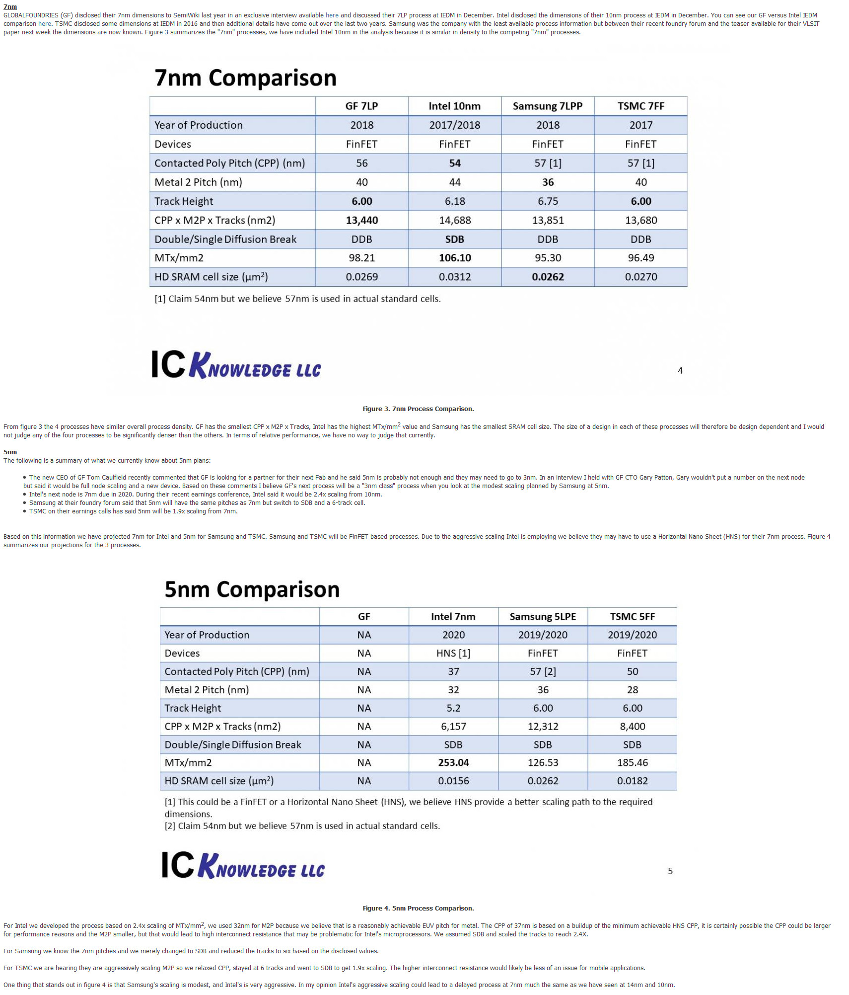
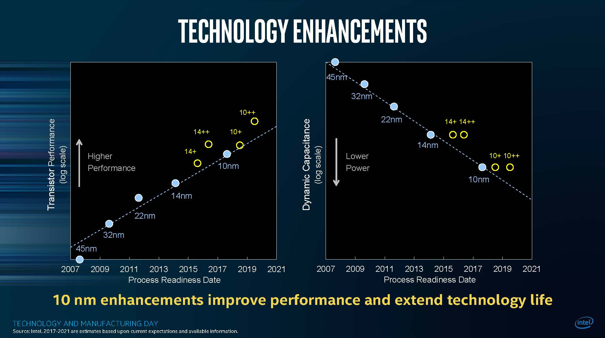
The ARM camps has for sure won the "perception" battle, at least the "nm" naming battle, those 2 slides are comparing and , on the top of this, non of those graph tell you about the Cdyn other important factors, or leakage at high voltage and low voltage, it is to compare

**Keep in mind that increasing IPC is not linear to the increase of transistors,the amount of IPC increase will depend on a lot of simulation, how accurate they are, and the scale of your R&D, this is where IPC increase is going.** Now,chipzilla has 3 years of architecture to release"

Important part there is that the architect supposedly warned Intel to pull in Ice Lake for14nm++ process a couple years ago, which was not listened to. He may be a bit hyperbolic and have strong statements regarding other fabs processes, specifically not looking at TSMC 10nm process, nor that 7nm is now in volume production. This statement was also made before Intel mentioned in Q2 earnings that 10nm chips would not arrive until Holidays 2019, and server in 2020, or that EUV is delayed until 2021. So, please do not judge the bravado or his strong stance on a former employer as misguided, when he made the statement, it was mostly true, considering 10nm TSMC doesn’t have the volume of 14nm, etc. But insight can be gained.

Intel’s issues come in defect densities related to SAQP, which is quad patterning, and certain decisions on cobalt (going to the smaller end for the same that every fab was looking at for their 7nm, which is equivalent to Intel 10nm density), contact over active gate (COAG), and on moving to a single dummy gate (discussed above in the iedm/isscc link, as well as the March 29, 2017 press day materials for their scaling). It is my belief not that the engineering is bad, just that the quad patterning is causing too many defects and that because of the physical limitations they are running into due to expecting EUV back in 2015 or 2016, they did not plan accordingly. So, insofar as EUV delay is involved, I do not fully blame Intel as EUV readiness was beyond their control. With that said, not changing direction or taking advice internally IS something that I can blame them for and will do so readily. No real excuse for not listening to those engineers and architects on the front line, so to speak.

Because of that, and EUV not being ready, and likely quad patterning or sextuplet patterning, and defect densities, I think Intel is removing some of the density to get it out the door, which is what semiaccurate has discussed and is linked, in part, above on the 12nm comments about Intel’s 10nm. With the rumors that it will be gutted to get out the door, with 10nm expected next christmas time frame (could be anywhere in Q4), and the announcement of not using EUV until 2021, we could see the Intel 10nm be a lesser process compared to 7nm at TSMC and potentially Samsung, but certainly after EUV adoption, which simplifies it from quad patterning and above down to dual patterning and allows for some designs that would not otherwise be possible. Intel then having EUV 7nm in 2021 needs discussed, such as whether it will keep the current density calculations or if it needs adjusted due to the gutting of 10nm. Intel’s 7nm is more comparable to around 3nm for other nodes, which also, coincidentally, meets the timelines for Samsung and TSMC, roughly, on getting to 5nm-3nm, meaning Intel may not ever have the process lead again, instead being on par with two other fabs that have larger volumes than Intel does.

But that gets into a discussion of the fight and timelines to 3nm, which should be discussed because that is where current means of producing chips breaks down, where we examine Gate All Around (IBM patented and Samsung has their own version), which can use nanowires and nanosheets, we examine III-V materials, copper trace doping, etc., to fight electromigration and quantum tunneling. This is the bleeding edge (along with nano-vacuum tubes, graphene (like learning how to inject the band gap, growing the film on substrate, etc.), optical interposers and light based solutions including photonic ram, quantum q-dot scaling and production on silicon transistor lines (great article on that, but I’d have to find it), and all that fun stuff). Other problems faced is cooling, stacking with TMV (through media VIAs, with through silicon VIAs being the most common to speak of), etc.

But, back to the point, Intel may be able to save it from doing a spin-off with the release of another high performant part, like the GPU they are planning for 2020-21. One reason they did not want it open in the past, and why competitors did not want to use it, was the process lead and the IP transfers needed to do so from all parties concerned. Now that the lead is gone, and may remain gone moving forward, the reason for keeping it close evaporates, which then requires keeping the production levels high while sinking R&D to be on the bleeding edge, etc.

But, I think I’m rambling now. Great points, hope this gives more context and information. Also, here is an article about cobalt and ruthenium in the new Intel 10nm chips, which continues the discussion on new materials and cobalt use. https://fuse.wikichip.org/news/1371/a-look-at-intels-10nm-std-cell-as-techinsights-reports-on-the-i3-8121u-finds-ruthenium/

1 Like

With the new iphones launched we will probably get a closer look at the A12 bionic chip soon, might give some more info on TSCM 7nm.

1 Like

Exactly my thought. Those are the first chips on 7nm, so first comparison on process advances. Now, there are tweaks between gens, so it would be good to try to tease out the difference on those as best as possible, but is nice. Around December, I expect AMD to show off Epyc 2 publicly, as that is Intel’s release of Cascade-SP/X. That should be the best comparison. Then Qualcomm Snapdragon (which will compare against 10nm prior version of snapdragon IIRC, which is supposed to be similar in density to the Intel 14nm, so it would see amount of performance beyond what an Intel equivalent node offers). Then, finally, released silicon.

Now, AMD did say consumer chips come after the server chips. So the question is whether AMD is doing full volume when releasing EPYC 2 sometime early in 2019, or if AMD will do a paper launch with low supply, then mainstream, then volume around computex, or what their exact roadmap is on that.