I recently created a blog where I write about projects and all sorts of things.
Here’s the first article where I wrote about creating a Socket 5 to Socket 7 CPU dual voltage adapter.
Also there is an overview of what more I’ve got going on
You can expect the next article this weekend. It’ll be a fun one.
Sometimes feeling out of place is common.
Most of the overall conversation on this forum concern gaming .
I am not an avid gamer.
But as someone who has been work centric all his life, task functionality is a key factor in life.
It’s not necessary to have the fastest or the shinier things provided they accomplish the task you want.
High Quality in tools means longer working life.
And makes a lot more sense economically
My contribution is not anything overtly special when it comes to gaming, but safety however is stressed to prevent damages to your equipment or yourself.
Consider the labor saving equipment.
Yes they may possible save a few aches and pains in under used muscles, but at what cost?
Over thinking and over engineering are common problems that affect everyone, not just the intellectual mind.
Sure it can be fun to design a highly technical solution.
But when compared with a simpler solution that can accomplish the task at less expense, How foolish does it look?
There are simpler alternatives if one just looks.
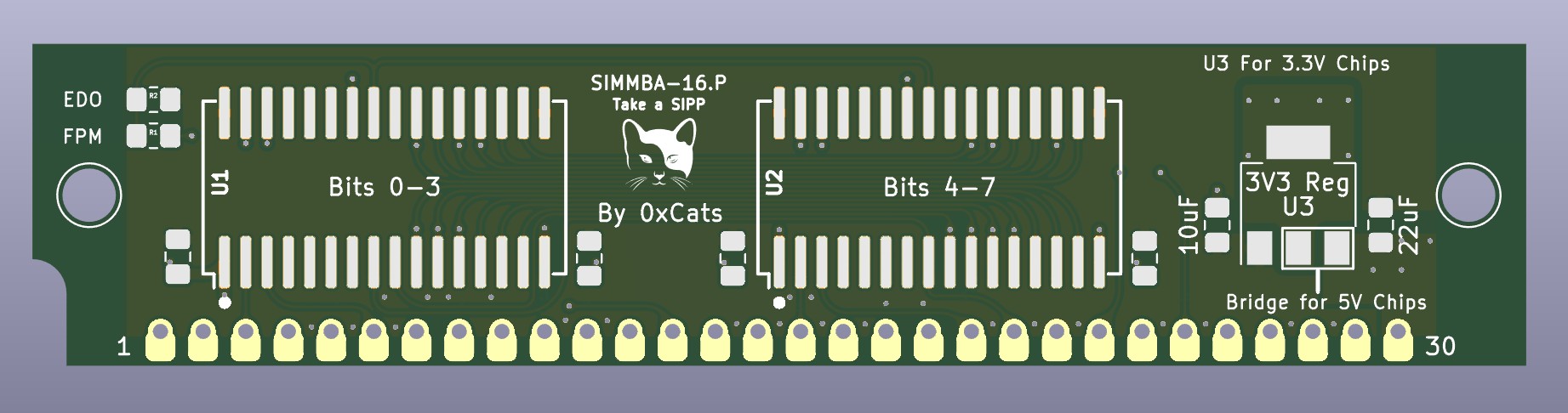
Just linking a project of mine here.
16MB 30 pin SIMM DRAM for your computing antiques.
Feel free to make them yourself or whatever you like.
Unfortunately it’s not economical for me to make these myself and sell them as I don’t have the time or logistics to deal with it.
They will however be very cheapo to make if you need some.
Have fun!
New levels of hardware chaos achieved!
Porting Coreboot to random old crap and breaking existing coreboot conventions in the process. Lots more to come from this in the coming weeks.
Turns out I need to write a new init stage for Coreboot to handle FPM/EDO systems.
Why is this? Well EDO and FPM RAM are not like SDRAM with it’s SPD eeprom onboard that tells you what the stick of RAM is and how it’s setup, how large it is etc. These old RAM sticks technically have a 4bit ‘size’ resistor strapping on them. But well turns out that’s a troll thing nobody’s been using since the IBM PS/2. Lines are not even connected on boards to the chipset.
So setting up EDO/FPM RAM involves just enabling one DRAM Row after another and writing into the void of memory space and checking until which address offsets you can successfully read back data. Then you program the memory controller ROW Boundary registers accordingly.
I liken this to measuring the boundaries of your house by running into the walls blindfolded, a bit like a roomba vac bot does.
And well turns out it’s not possible/reliable to run the memory scan algorithm with L1 cache enabled since the scan algorithm ends up clobbering the cache lines and we need those to store Stack during the Cache as RAM stage in Coreboot XD.
So I need to do memory scan with L1/L2 everything disabled really early during power up.
This is a bit problematic since Coreboot usually relies on the CaR (Cache as Ram) stage fairly early before memory setup is done. Sine that also gets you proper stack and real mode calls
Usual mode of coreboot startup:
System booting begins, and the CPU starts executing the reset16.inc code. It then jumps to entry16.inc.
In entry16.inc, the system switches to 32-bit protected mode, enabling access to advanced processor features.
cache_as_ram.inc is executed, which initializes the CPU cache and prepares it for stack usage.
cache_as_ram_auto function in auto.inc is executed and runs northbridge init and dram setup.
post_cache_as_ram is executed. It copies the stack from the cache to RAM, sets up a new stack, stops the cache_as_ram process, and clears the first 1MB of memory for hardwaremain. It then calls the copy_and_run function.
The copy_and_run function copies or unzips the hardwaremain code into RAM and jumps to it.
The hardwaremain starts from c_start.s and calls the hardwaremain function, which continues the boot process.
Now I have two ways of doing EDO startup: Method #1
System booting begins, and the CPU starts executing the reset16.inc code. It then jumps to entry16.inc.
In entry16.inc, the system switches to 32-bit protected mode, enabling access to advanced processor features.
dram_scan.inc execution which runs chipset specific DRAM row boundary scan code and stores the DRB return result in 8 registers.
cache_as_ram.inc is executed, which initializes the CPU cache and prepares it for stack usage as well as slaps my 8 register values into a cache line for temp storage
cache_as_ram_auto function in auto.inc is executed and runs northbridge init and dram setup using the newly available pci_write functions to setup the DRB’s from the cacheline address
proceed as normal before
Method #2
System booting begins, and the CPU starts executing the reset16.inc code. It then jumps to entry16.inc.
In entry16.inc, the system switches to 32-bit protected mode, enabling access to advanced processor features. (this is required to get Gate A20 setup for full dram access)
custom dram_scan.inc execution which runs chipset specific DRAM row boundary scan code and programs DRB using assembly legacy IO port routine.
run standard cache as ram routine and proceed as normal.
To be honest I think the only realistic way to do this will be Method #2 to use the chipsets DRB registers themselves to store the DRAM boundary scan result rather than the L1 cache prior to Cache as Ram stack setup, because then I need to change the CaR code to handle this
Or instead of storing the parameters in the chipset registers directly I slap it into the 128 bytes of CMOS storage I’ve got available via legacy IO port writes. That way I can also re-use these if RAM setup has not changed after a reboot.
Though all of this kinda makes it difficult to propagate information about potentially memory errors detected during EDO boundary scan forward since there’s not really anywhere safe to store lots of details from the memory scan stage.