Just something from days past.
How low have you ever underclocked a graphics card?
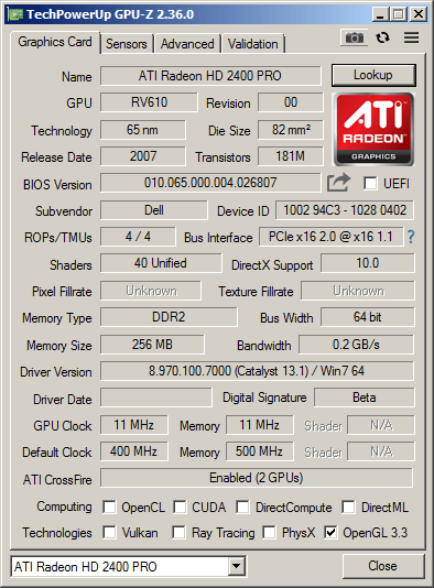
Lowest I got it with 2D clocks still functional was 11Mhz. 3D was toast.
The lowest ever benched on a HD2400 crossfire setup was done at 60Mhz and was stable enough to complete a run of 3dmark 2006. Very very slowly.
3Dmark 2001 SE gave interesting results.
This is an FX5200 (64bit) PCI card. The slowest FX card mankind was ever cursed with. GPU-z optimistically lies to me and says it’s 128bit.
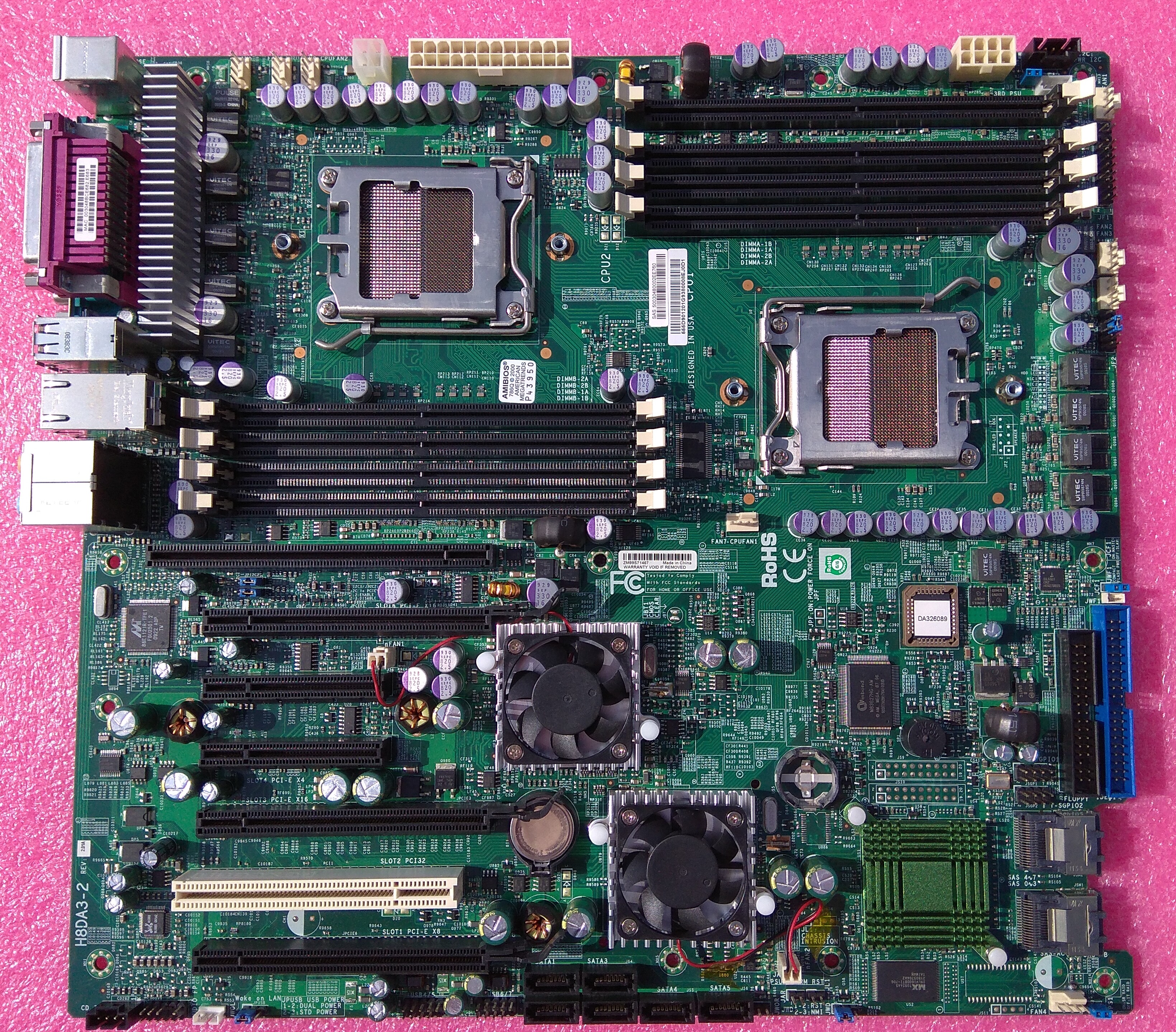
It joins my other Dual Socket F board the MSI K9ND Speedster 2 aka (MS-9661).
But unlike the speedster 2 this Supermicro has a far nicer VRM and more PCI-e lanes. Since they used 2x MCP55 (nForce 3600 Pro) chipsets linked to the primary processor HT bus.
VRM on this supermicro is made of a pile of Infineon OptiMOS BSC020N03LS mosfets. 3 per phase to be specific, which is hilarious overkill. It has them on the back and front of the board.
The manual is selling this board a bit short. Realistically you can push close to 200A with some air cooling.
Also the chip-to-chip interface is bi-directional and clocked at 2Ghz with processors I will be using. Two times Opteron 8435. With a total of 32GB of DDR2-800.
Small question, where did you get the block diagram from? It is public knowledge, like from the manual, or do you have a tool that generates this for you?
A fully dynamic spreadsheet detailing the internal operating parameters and programming constraints of ATI HD 5000 and HD 6000 GPU’s as of now. These are GPU’s that I am very familiar with.
Features
ATI HD5000 and HD6000
if you change the ram or core clocks or memory bus widths etc it will update to show you all the new internal bandwidths and Global Limits
You can clone it to your own drive or download and use it almost as a build a custom Terascale GPU
Cons
I have not yet put in stuff like the firepro cards or IGP’s
Just original ATI (AMD) ASIC definitions
There’s a good few ‘magic constants’ involved for the register math and global limits that I don’t reveal.
Still missing GCN and RDNA (soon to come)
Notes
A lot of the IGP’s use the HD5450 core model. The math for which can sort of be extracted from the sheet formulas. HD5450 is also special and has lots of shortcuts in the cache and LDS/GDS design.
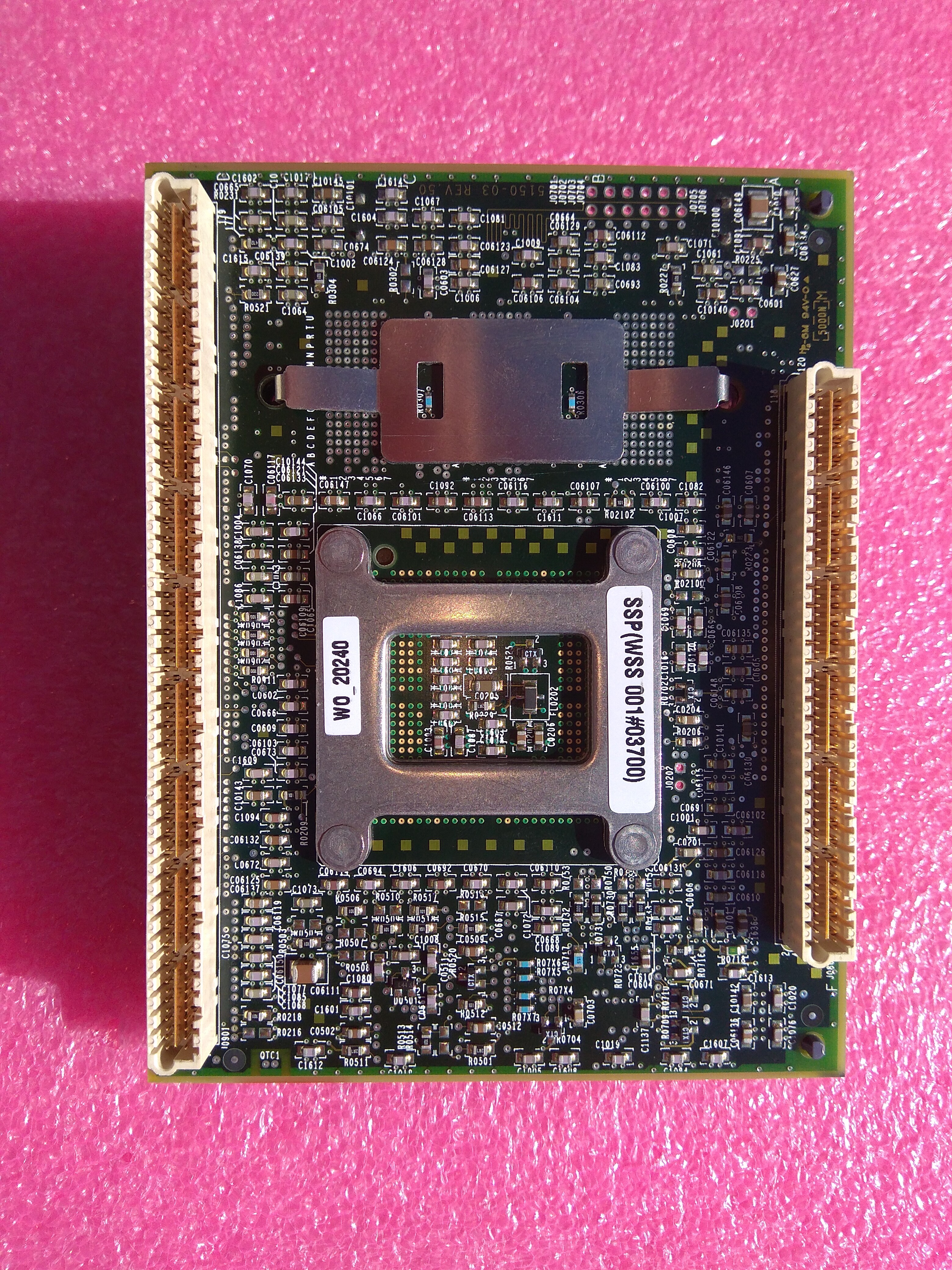
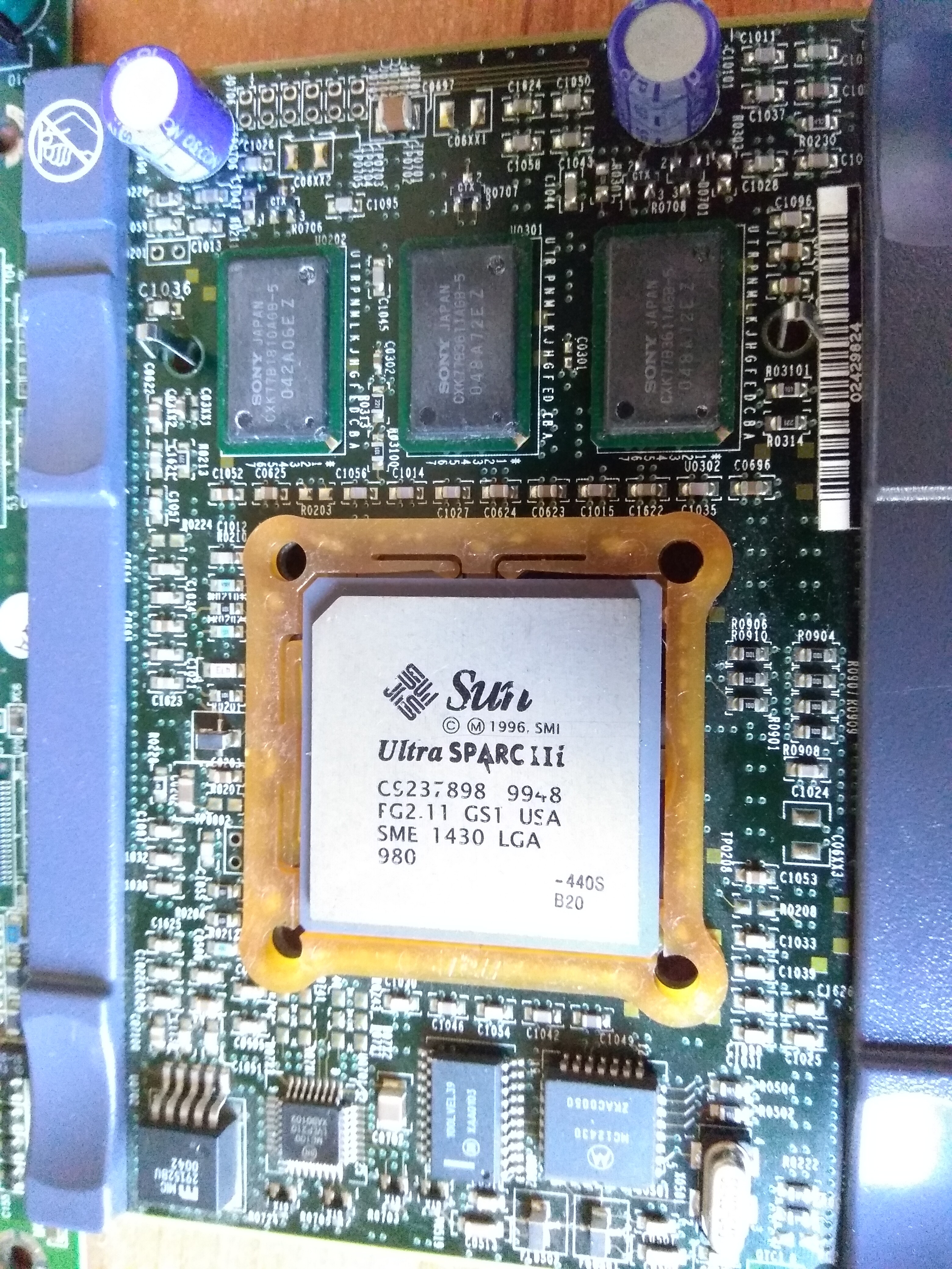
Here’s a SUN Ultra 10 (Model 375-0009) motherboard equipped with the Sapphire Red 440Mhz 2MB L2 Cache SUN UltraSPARC IIi processor (Model 501-5149).
It’s not actually directly compatible without some extra mods and I’m still waiting for the correct CPU (Model 501-4379) 300Mhz Sabre with 512KB L2 Cache.
It uses a Flex PCB sheet with what seem like solder bumps. But these aren’t your normal tin solder. It’s something else much harder. The sheet can be removed to show the pads underneath.
Any suggestions for what I should do with this thing once it’s up and running?
Probably gonna be running Solaris 8 in the as shipped configuration first.
There will definitely be some micro benchmarking and linux kernel hacking done. But also I have plans to game a bit on this box. See what I can cross port to this architecture since it has a dang powerful FPU/Integer pipeline.
Think like Pentium 3 1Ghz, but we’re trucking at 400Mhz.
For example on x86 Pentium 3 a FDIV takes 39 cycles and does not pair well with Integer operations.
The FPU tho doesn’t mess around, almost all operations are fully pipelined and occur at 1 per cycle. Even 64bit, (this is a 64bit processor)
Divide and Square root are not pipelined, and take 12 cycles single precision or 22 cycles double precision. But interestingly also do not stall the processor. Follow up instructions can be issued immediately. Integer and FPU pipes are synchronized. Performance magic that the pentiums could only dream of because any other instructions, following the divide/square root can be issued, executed, and retired to the register file before the divide/square root finishes.
On the other hand Pentium Pro and Pentium 1,2,3 can’t do what the SPARC does and have horrible constraints on how you can sequence and pair Floating point and Integer instructions.
And all that with just 5.4 Million transistors vs the 9.5 million of a 500Mhz Katmai core. L2 cache transistor count for both is not included.
Also fun fact:
The 64-bit SPARC V9 architecture uses big-endian instructions, but can access data in either big-endian or little-endian byte order, chosen either at the application instruction level or at the memory page level (via an MMU setting)
I’m personally always interested to see some benchmarks comparing different CPU architectures, even tough it’s always apples to oranges comparison. And it’s also fun to see someone play games on hardware that wasn’t built for that purpose.
Oh hi there.
Things have just been busier in the past year or so plus.
Changed line of work, took on new senior roles.
Spent some time away as well, all those interesting things in life.
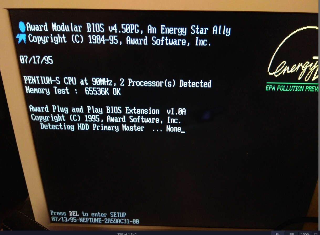
Finally go the SUN Ultra 10 board up and running with a Sabre 300 CPU.
This is board 375-0009 and while the 440Mhz Sapphire Red CPU works on it, I need to update the boot rom first and fix some things on the processor card to run stable.
This is just a bit of a bumbling video of me talking about the board and what was wrong with it.
It took me a second of wondering how to mount the cooler without mounting holes. Then I remembered. Oh, I remembered. On an unrelated note I find it tempting to try to test of how far back in time I can go hardware wise and still let the newest Linux kernel run on this old piece of tech. But I do not have the space to store ancient pieces of hardware like the ones you posted for a project like this. Every new thing I get these days bothers me, because I want to have a small footprint.