We know TR2 and 32 cores is a thing coming next quarter. It has some bottlenecks like quad channel memory will only feed into 2 of the 4 chips with infinity fabric shifting data after that. Will be some memory limitations on heavy workloads.
Now Zen2 @ 7nm. Very little was said other than the hints of halving / doubling etc. So I can see the next EPYC CPU’s could double. So next year 48 and 64 core EPYC chips.
That means TR3 next year can be a 2 hot + 2 dead chip 7nm fab. No memory limitation and the power / speed gains from 7nm.
Ryzen 3xxx can be 7nm as well can potentially hit 16 cores.
They have. And since their 10nm isn’t really going well they are considering breaking down the chip to modules and manufacturing with different processes… Adored talked about that a few days ago.
Basically the cores would still be 14nm, while memory controllers and other stuff will be a separate dies and could be made on 10nm.
But that is crazy speculation…
Ryzen 3000 is confirmed at 7nm… Now the question is, will they increase the complex from 4 to 6 core and make 12 cores max, or will they just add another die complex, basically adding a second 8core to the first 8core.
I think they will just have 12 core. I mean they now have 2 dies, 4 cores each. They will either make the dies 6 cores instead of 4 cores or add another die and make them 3 dies 4 cores each…
I’m not familiar with 7nm specific, but doubling the core count effectively may raise massively the power usage and some of those cheap B350 boards with 3 phases VRMs… They will not survive. But I can see raising the core count with 50% without really moving the power draw at all. Heat as well… I mean I don’t know, but 16 cores is a bit too much to expect IMHO.
Me either but when I see the power regulation changes in 2xxx over 1xxx chips. I can totally see the 7nm chips having power envelopes to throttle automatically in older boards and or power / temp constraints.
The 2700X is basically max overclocked out of the box.
7nm also does lower power draw as well as letting you add more transistors.
Id welcome experts because I am not one. I try to hover up information nuggets to put together.
What’s interesting about GF’s announcement is that it’s also claiming up to 60 percent reduced power with 40 percent improved performance.
So basically just optically shrinking Ryzen to 7nm will basically halve the power draw and add up to 40% performance, effectively killing Intel, because at 7nm it will be cheaper, faster, cooler and will use WAY less power…
And that is just a shrink from 14 to 7. No architecture improvements.
Short term Intel might take a hit, but they are also very busy with 7nm EUV. GloFo and TSMC might be the first, but eventually intel will have a whole fab available for themselves and AMD will have to share the EUV machines with other customers of TSMC and GloFo. At some point their installed base will probably surpass that of Intel so availabality wouldn’t be an issue anymore, but untill thats happens Intel will take the advantage prob.
Its definitely going to be a couple of interesting years.
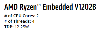
I’m curious of what AMD has for the lowest end embedded and see how useable it is going forward. Every now and then, I compare the lowest end CPU of today and compare it to a CPU from a time where the highest end CPU had similar performance.
Because if the lowest of the low is very usable, that says a lot to everything else and how far we have come.
At the low end I think phone CPU’s rule the roost. Cant beat lean CPU pipelines. But while closed source and AMD64 instruction sets is king. We have the core wars, Intel and AMD.
As soon as AMD64 CPU’s is off the table APPLE is king and everyone better get ARM asap.
We are holding on to a CPU like Windows. That is so old it should be dead.
I’d rather have native compatibility to support VMs. Also don’t those Windows on Arm Devices have locked bootloaders so you can’t install Linux on them?
I’m not sure x86 is a truly secure platform anymore. In time arm will do x86 VMs at a reasonable speed.
The locked bootloader is just an annoyance. It doesn’t have anything to do with the underlying technology.
If you want to be pedantic, technically parts of the x86 instruction set doesn’t even exist anymore. The instructions get decomposed into other instructions. It’s neat.
As far as I understand it ARM can’t really scale up (yet) to the kind of high performance you need on the desktop and x86 can’t be scaled down to be any good in efficiency for mobile, right? So a unified architecture for everything is still pretty far away but since all attempts to use x86 in mobile failed, the only way to go is to beef up ARM.
welll… its slightly more insane than that. The limitations that we’re up against at this point are basically speed of light problems. If we make a compute core smaller, we can clock it way up because we don’t have to wait for signals to propagate from one end to the other. If arm adds a lot of instructions/compleixty, upclocking it will be hard just because of the length of the wire and the transistor settle time.
Similarly, intel can’t add too much more complexity without things getting weird. So we have things like avx-512 now which really does speed things up dramatically but for all intents and purposes it is a totally separate isolated independently clocked compute unit.
Arm could do something like that. Probably we’re entering an age of heterogeneous silicon simply because there is not much more low hanging fruit. We’ll see 22nm memory and 14nm compute cores and 7nm interconnects probably all mixed together. Possibly we might see some avx-512 type computation actually on dram in the near future? but probably nothing fast since that’ll take a special compiler.
I am blown away by how much x86 compatibility there is, but how physically small the ryzen compute die is. I would love to know what’s going on there. AMD has pulled a rabbit out of a hat. And remember from the pcper benchmarks the corner-to-corner die latency was measurably worse than adjacent ccxes… and much worse than ccx-to-ccx latencies. Intel’s still got this dual ring bus in some cpus but they’re moving to the same silicon.
So if arm scales x86 by having an x86 translation core? Then it could be an almost overnight thing. Because I’m betting inside zen they break down at least a good portion of x86 instructions into sequences of micro-ops that make more sense in a modern world. Arm can do the same thing and it’s basically “only” a pipeline modification. Transmeta published some nifty papers on this way back in the day.
Someone I think took pictures of the sandy bridge silicon and overlaid that on cpus up through kaby lake. and it was the same looking in the photo compute core surrounded by more and more silicon for specialized functions added in haswell, skylake, etc. It was scary how little had changed and how much was just “added on” as specialized compute cores.
hbm cpus is probably the next thing with dram used as a sort of secondary ram cache I bet. Or possibly a new form factor where you inject hbm somehow into a ceramic cpu carrier manually. That’d be neat. I should patent some obvious ways of doing that… think of an old school looking cpu like ta pentium pro or threadripper with “micro sd” looking slots for hbm on them. lol.