For Threadripper, first generation, and even only the 8-core version at that. All other processors and subsequent platforms/processor that came after that were all more expensive than that.
Moreover, the 7th generation processors from Intel was the last generation that had (in the Core i9 series) that had 44 PCIe lanes and commanded about a $300 premium over the launch price of the Threadripper 1900X.
How fucking stupid is THAT???
That’s LITERALLY NOT what this OP is about.
Read the fucking title of this OP.
All I am asking is where can I find the information necessary to be able to calculate the theorectical peak memory bandwidth.
That’s it. Period.
I LITERALLY told you that I KNOW that the Ryzen platform only has anywhere between 20 to 24 PCIe 4.0 lanes, but that’s NOT what my OP is about.
Again, literally, re-read my OP.
The ib_send_bw results show 96.58 Gbps (out of a theorectical 100 Gbps available, which I tested and blogged about it here: Tech in Wonderland: Welp....this is a problem.), so contrary to your claim and assertion that I am “complaining” about the Ryzen NOT having enough bandwidth, is patently false, per my blog post. (and that isn’t what this OP is even REMOTELY about).
Again, as I’ve stated, the question here is LITERALLY: “Where can I find the chiplet-to-chiplet theorectical peak memory bandwidth limit for AMD Ryzen 9 5950X?”
NOWHERE, in the OP, (or anywhere for that matter) do I complain about the lack of bandwidth, because what I actually talked about was the fact that a) I CAN’T install the discrete GPU in the secondary PCIe slot. The system/platform/BIOS won’t let me. (If you install the discrete GPU in the secondary slot, during POST, it will actually show you an error that tells you to install the discrete GPU in the primary slot, and the system won’t boot with said discrete GPU installed in the secondary slot. That’s not a complaint. That’s just a statement of fact.
Which means that if I want display output, I need to expend a PCIe 4.0 x16 slot for a Nvidia Quadro 600 which is a PCIe 2.0 x16 card. (Source: NVIDIA Quadro 600 Specs | TechPowerUp GPU Database) Compare that to the upcoming AM5 platform where all of the CPUs will have SOME form of an integrated GPU, which means that for this kind of a basic video output, I won’t have to expend said PCIe 4.0 x16 slot on a PCIe 2.0 x16 GPU. Again, that’s not a complaint. That’s just a statement of fact.
The “so what?” of that is that if I want my Mellanox ConnectX-4 (MCX456A-ECAT) 100 Gbps Infiniband card to have access to the full bandwidth (as it is a PCIe 3.0 x16 card), I would have to forego having ANY sort of display output/discrete GPU installed, and run the system completely headless, which I’ve been able to do, successfully, for about a month now, without any issues. That’s also not a complaint. That’s just a statement of fact (in terms of the operational state of the systems).
The question isn’t about whether it has or doesn’t have enough bandwidth. The question is “what’s the chiplet-to-chiplet theorectical peak memory bandwidth?”. That’s LITERALLY the question that I’ve asked in the OP, which again, clearly, you need to re-read again. (Which I literally copied-and-pasted the bandwidth data that is printed to the solver output file.)
AMD’s own technical presentation tells you that the write speed between the IF connector on the CCD to the IF connector on the I/O die can write at 16B/cycle (128 bits/cycle). Since I am using DDR4-3200, and if the Infinity Fabric is also operating at “3200 MHz”, then it would be able to support 409.6 Gbps. But if the IF is actually operating at HALF the speed, then the maximum bandwidth that it would be able to support would be 204.8 Gbps.
At 3.2 GHz, that means that you have a cycle every 0.3125 nanoseconds.
At 1.6 GHz, that will work out to a cycle every 0.625 nanoseconds.
But if the latency is 17.0 ns, the maximum cycle rate is 58.82 million cycles/second.
The results that printed by the solver to the output file shows that on the same CCD/CCX, the bandwidth that can be attained, on average, is 23993.6329 MB/s, which is 93.725% of the theorectical limit of DDR4-3200 through the Infinity Fabric (204.8 Gbps or 25.6 GB/s = 128 bits * 1.6 GHz)
So within the same CCD, the math theory appears to work out. (@93.725% that’s actually attained by the solver, as indicated from the solver output file, that’s pretty close – it indicates that it is making good use of the available bandwidth (limit).)
By running the calculations backwards based on the bandwidth that’s printed to the solver output file, with an average of 7707.1045 MB/s, and assuming the same “efficiency” of 93.725%, that means that it the “theorectical” bandwidth would be 8223.1043 MB/s.
And then back-calculating what the frequency would need to be in order to achieve that with the same 128 bit wide interface (16 bytes/cycle) would be 513.944018404908 MHz. And that would correspond to a latency of 1.94574E-09 seconds.
I have no idea if that’s even remotely close to being correct according to the theory.
Hence the reason for my question.
Nowhere in my OP do I “complain” about it given the OP was about how to actually perform this calculation based on theory, and whether this is even the correct arithmetic procedure (or not).
The purpose and the entire point of this post is to check and see whether the arithmetic procedure is correct, proper, and appropriate for this kind of calculation; and if I have err in the arithmetic process, how do I fix and/or correct it; which is the point of this OP. You have contributed NOTHING with respect to this OP that’s remotely close to this point and purpose.
No, it’s more “classical”/“traditional” computational structural mechanics.
It doesn’t use any AI/ML at all during the Newton-Rhapson solution process.
I’m not sure what nor how the sparse matrix solve actually stores the data, to be honest. There’s a potential that due to the symmetry of the matrix, it might just store half of it (so, it might go through some kind of LU decomposition, and then just store the upper half possible in COO format), but I can’t say with any certainty what the internal works of said sparse matrix solve actually does nor how it works. It’s not documented in the theory guide that’s published by the software ISV.
Yeah, I’m not really sure how well TF and/or TPUv4 ML will be able to handle the combination of non-linear geometry, non-linear materials, and non-linear contacts simultaneously.
If it my understanding that typically, to be able to even TRAIN this kind of an AI, you’d have to be able to feed it enough cases so that it would be able to relate outputs to inputs. But the problem with that is if you changed the geometry, then you’ve changed the outputs. Topology optimisation is the closest that I’ve seen to this kind of solution technique whereby you tell it, for example, what is the maximum von Mises stress that your part is allowed to incur, and then it will progressively remove material until it hits that limit, and that would then suggest what your new design might potentially look like. (And you can add in, for example, manufacturing constraints in order to constrain said topology optimisation problem, which changes how it arrives at the solution to said topology optimisation problem.)
It would be nice and/or interesting to be able to use TF/AI/ML to be able to solve computational structural mechanics problems this way.
I think that training the model, because it is dependent on solutions like the one that I am currently solving for, as the data that you would feed into said TF/AI/ML training model for it to work itself out, and that further assumes that the resulting TF/AI/ML computational structural mechanics solver would be general enough that you would be able to apply it to subsequent problems, even if those problems are vastly different than what you trained the model with, or that you might need to general sub-models for each sub-class of problems that you wish to solve (which is a little like how OpenFOAM works, albeit, it’s not TF/AI/ML, but you have to manually call a different solver for each different type or class of problem that you are trying to solve, vs. having one solver executable, and it just has flags or switches within that single executable to activate or deactivate the parts of the solver that you need or don’t need.)
Yeah, so my other thought to this is actually a little bit of a variation (of sorts) on this them.
We’ve seen that a single CCD actually performs really well in terms of communication bandwidth and/or the lack of latency (or super low communication latency). Therefore; one idea was actually instead of connecting a bunch of higher core count CPUs (like 16 and 32 or 64 core Threadrippers/EPYCs together), one idea was to actually link together a bunch of 8-core systems (e.g. Ryzen 7 5700Gs) and then have that form a (Beowulf) cluster to do the same thing. That way, each node can actually be relatively very low power, and all you would really need is the single PCIe 4.0 x16 slot that you can get say from an ITX board or something along those lines, and then you can deploy a bunch of those nodes such that each node will only have a single CCD to contend with.
Again, at least that’s the theory.
The added expense would come in the form of needing to buy double the number of Infiniband network cards, plus the cables to go with it (as I already have a 36-port Mellanox 100 Gbps Infiniband switch running in my basement, so that’s not an issue).
But that would be another way to go about this.
I don’t know if that would be any better and/or any faster, but that’s why it’s a proposed theorectical solution to this question/problem. No idea if this will work according to the theory or not. (Most likely not. You get MPI communication overhead.)
So yeah…there are different solution paths, and it’s optimised against cost and SWaP.
your sure you have the correct type of memory interleaving set for your cpu.
in my uefi there is an option to change how interleaving is handled depending on how you populate the ram slots. and what interleaving your ram supports.
one of the settings may enable you to share the memory evenly between all cores instead of the majority of the bandwidth going to 1-7
*edit
I’m going to make this REALLY simple for you:
You said: “The Latency fore Core 0 to Core 16 is because Core 16 is a virtual SMT Core.”
And I’m asking you “WHERE are you getting that from?”
If your argument had ANY technical merit, we would’ve known by now because you would have GLADLY, EASILY, and READILY shared it.
But you haven’t.
This is the simplest way to tell that you’re completely full of shit.
The rest of your bitching is because you finally got caught with your BS and you’re pissed about getting caught rather than being pissed that your argument lacks ANY technical merit whatsoever.
And since you aren’t man enough to take responsibility for your own argument, lacking ANY technical merit; which means you can’t get mad at yourself, you, therefore; bitch at the messenger who caught you instead.
Why don’t you ask yourself why you weren’t ready, able, nor willing to defend your own argument on its own TECHNICAL merits?
Did you EVER bothered to ask your own self, that question???
Maybe you should try that sometime instead of bitching at the messenger for why you are so ill-prepared to defend the arguments that you’ve made.
It’s literally THAT simple.
I thought that you said that you were done?
LOL…LMAO…
Once again, clearly, you’re not.
It ain’t my fucking fault that you can’t seem to defend your argument.
LOL…
NOTHING that you have written even REMOTELY resembles “helping” or trying to be “helpful” in ANY sense of those words.
You LITERALLY wrote:
When asked where’s your source for this, you STILL haven’t been able to provide a SINGLE source that corroborates this statement.
The fact that you’re dumb enough to make a statement and then FAILING to provide ANY sort of supporting documentation/data/evidence to support and backup the statement that you’ve just made is entirely your responsibility. You should have learned that in elementary school.
(See kids? THIS is why you should stay in school, so that you’d learn how to make a point and then defend it with ANY, ACTUAL sources to backup your claims.)
Don’t blame the fact that you can’t fucking defend the bullshit that you’re saying on me.
I’m not the one who’s making the claim that:
You are.
You said it, therefore; it is up to you to defend your own statements.
This is very simple.
The fact of the matter is that you made a claim.
And when asked where is your source that forms the basis of this claim, you have repeatedly fallen short and utterly and completely FAILED to provide any sources and/or citations which backs up the claim that you made.
It ain’t my fucking problem that you’re completely incompetent.
You make the claim, you are responsible for providing the sources, citations, data, and evidence to back up your claim.
Failing to do so will result in your claim getting called out as bullshit which is PRECISELY what happened here.
You’re just pissed that you finally got called out and that what’s probably worked for you up to this point as you skate by with in life, FINALLY doesn’t work anymore and it all comes crashing down on you as your bullshit (and your claim being subsequently being called out for the bullshit that it is) – you’ve been able to get away with it for so long that when you finally meet someone who’ll call BS on the claims that you’re making that you’ve demonstrated that you can’t defend – you don’t know what to do with that BECAUSE you’ve been able to get away with it for so long.
So, what do you do?
Instead of ACTUALLY trying to find a source or citation that you can provide/share with everybody here that actually speaks to your claim, you; instead, proceed with the employment of the ad hominem logical fallacy and the tu tuoque logical fallacy.
But the reality of your argument still remains in that you have STILL yet to provide ANY sources or citations that backs up the claim that you initially made.
That’s the reality of the situation here.
You can bitch about me all you want.
It doesn’t change the fact that your complete and utter incompetence has FAILED to provide ANY documentation, ANY evidence, ANY sources, nor ANY citations that supports the claim that you’ve made.
And the saddest part of this ENTIRE exchange is that I’ve EXPLICITLY pointed this out to you by repeatedly asking you to show me where you got your information from and you have REPEATEDLY failed to do so.
That’s an entirely you problem.
I’m not responsible for proving your claims.
In fact, everything that I’ve supplied here - you have been able to argue precisely NONE of it on ANY technical merit.
You make claims.
You don’t provide ANY data/evidence/sources/citations to back up your claims.
I provide more data/evidence/sources/citations to back up my counter arguments against your claims.
And the BEST that you’ve been able to do is ignore the data.
That’s it.
Here is the clear and concise example of the internal inconsistencies about your own argument where you wrote:
To which, you followed up your own argument with your own statement:
You LITERALLY said that crossing the I/O die will incur a latency penalty.
And then you turn around only to argue against yourself by saying “If you are using only 16 threads instead of 32 and are still hitting the latency penalty then you have either uncovered a design flaw or you are doing something wrong.”
Yet, you LITERALLY ADMITTED to the fact that crossing the I/O die will incur a latency penalty.
So which is it?
This is a PERFECT example of the type of internal consistency within your own argument that I am talking about, and you STILL haven’t been able to rectify nor resolve this.
In what fucking universe does your bullshit responses which aren’t even internally consistent “helpful”???
LOLLL…
If you were ACTUALLY able to provide sources and citations to the claims that you were making, then I would be able to READ your sources and actually LEARN something from them.
But being that you have made it your mission NOT to provide any, and you have completely and utterly FAILED to provide ANY sort of technical explanation as to why the solver output LITERALLY tells you that the communication latencies are:
Latency time from master to core     1 =    0.495 microseconds
Latency time from master to core     2 =    0.473 microseconds
Latency time from master to core     3 =    0.472 microseconds
Latency time from master to core     4 =    0.466 microseconds
Latency time from master to core     5 =    0.464 microseconds
Latency time from master to core     6 =    0.469 microseconds
Latency time from master to core     7 =    0.466 microseconds
Latency time from master to core     8 =    0.707 microseconds
Latency time from master to core     9 =    0.710 microseconds
Latency time from master to core    10 =    0.723 microseconds
Latency time from master to core    11 =    0.710 microseconds
Latency time from master to core    12 =    0.713 microseconds
Latency time from master to core    13 =    0.710 microseconds
Latency time from master to core    14 =    0.716 microseconds
Latency time from master to core    15 =    0.709 microseconds
Where the average latency from master to the cores on the first CCD/CCX is 0.472143 microseconds and the average latency going from master to the rest of the cores that are on the second CCD/CCX is 0.71225 microseconds – the data and the results LITERALLY show that traversing the I/O die WILL result in a latency penalty (which you have correctly stated); which is in DIRECT contradiction to your own other statement that you’ve made:
Like, how the FUCK do you NOT get that???
The data LITERALLY shows this, black-and-white.
I don’t have to do anything special or unique to it.
The solver from the software ISV who wrote it TELLS you this.
Dr. Cutress and Andrei Frumumasu tells you this.
AMD themselves, tells you this.
You don’t want to read those sources so that you can learn from it – that’s your fucking perogative.
But if you don’t WANT to learn from it which results in you being continually wrong, and as a result, getting constantly called out for it – that’s on you.
The fact that you can’t back up ANYTHING that you’ve said with data/evidence in this data-driven, evidence-based discussion – that’s on you.
You’re only bitching at me, the messenger, because you’ve finally been caught and you LITERALLY don’t know how to respond/react to it, so instead, you yell at the messenger, when in reality, the person who is responsible for your own actions is you.
You don’t want to learn, that’s on you.
You can’t cite your sources, that’s on you.
I’m only the one who’s willing to call BS on you because presumably no one else in your circle is willing to.
Your statement hypothesises that the virtual cores (i.e. logical cores/threads) has almost a 5x latency compared to the “physical” cores (they’re ALL physical cores because they ALL use physical hardware), and yet, when I presented the analogy to you re: the right arm talking to the left arm, you have REPEATEDLY and CONSISTENTLY FAILED to explain your hypothesis as to why your right arm talking to your left arm will incur an almost 5x latency penalty vs. your right arm talking to the right arm of the FURTHEST person that’s standing across from you.
That’s LITERALLY the claim that you are making.
And you have FAILED to explain how that can be REMOTELY, PHYSICALLY possible.
This is the kind of shit that forms the basis as to why I am calling your BS out on you (and this is in addition to the fact that you’ve repeatedly FAILED to provide ANY data or evidence that supports this hypothesis of yours).
It’s literally me asking you “how on EARTH is that suppose to work, PHYSICALLY?” and you can’t seem to answer this very simple, basic question.
That’s on you.
If you can’t defend your own fucking claims, that’s your fucking problem.
LOL…LMAO…
And yet, you have FAILED to provide ANY data nor evidence nor have you provided ANY correction to ANY of the arithmetic and/or solution methodology that I have presented here.
You can talk shit all you want.
At the end of the day - that’s ALL you are, is full of shit and no substance.
If you had ANY data or evidence to share, you would’ve shared it by now.
If you thought that my solution methodology and/or arithmetic was incorrect in any way, shape, or form, you would’ve GLADLY pointed those out to me by now.
And yet, you’ve done NEITHER of those things.
LOL…
Bitch please.
I’ve read more in this thread than you have.
How the fuck do you think that I sourced and cited my sources and citations, dumbass???
LOL…LMAO…
Get over yourself, you fucking tool.
LOL…LMAO…
GigaBusterEXE tried to help before you “attempted” to.
(And let’s be real here - NOTHING that you wrote REMOTELY helped at all. The question is super simple. And what do YOU end up talking about?
You come up with this shit instead.
Dr. Cutress and Andrei Frumumasu LITERALLY wrote, in DIRECT contradiction to your claims:
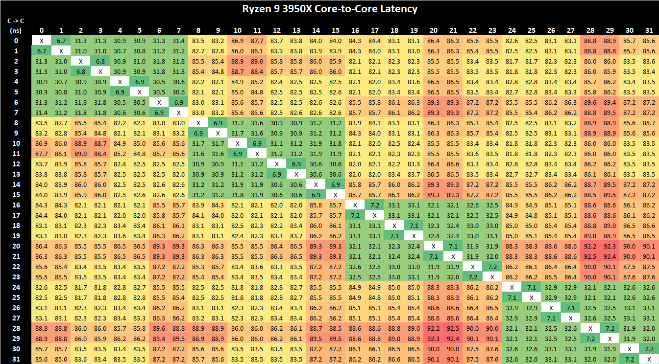
"Nevertheless, in the result we can clearly see the low-latencies of the four CCXs, with inter-core latencies between CPUs of differing CCXs suffering to a greater degree in the 82ns range, which remains one of the key disadvantages of AMD’s core complex and chiplet architecture.
On the new Zen3-based Ryzen 9 5950X, what immediately is obvious is that instead of four low-latency CPU clusters, there are now only two of them. This corresponds to AMD’s switch from four CCX’s for their 16-core predecessor, to only two such units on the new part, with the new CCX basically being the whole CCD this time around.
Inter-core latencies within the L3 lie in at 15-19ns, depending on the core pair. One aspect affecting the figures here are also the boost frequencies of that the core pairs can reach as we’re not fixing the chip to a set frequency. This is a large improvement in terms of latency over the 3950X…Inter-core latencies between cores in different CCDs still incurs a larger latency penalty of 79-80ns, which is somewhat to be expected as the new Ryzen 5000 parts don’t change the IOD design compared to the predecessor, and traffic would still have to go through the infinity fabric on it."
The fact that you have repeatedly and consistently REFUSED to read – that’s not my fucking problem. Sounds to me like that’s yet another you problem.
Their core-to-core latency plots (for the 3950X) which shows the >2 CCX architecture of Zen2 latency (which would reflect the architectural layout of your 3900X which has 4 CCXs * 3 cores/CCX in two CCDs and your Threadripper 3960X which has 8 CCXs * 3 cores/CCX spread over 4 CCDs) would exhibit a similar latency pattern: within the CCX/CCD, you would get the lowest latency. But once you need to traverse the I/O die, the latency increases.
Again, the source from Anandtech tells and shows you this:
The fact that you are LITERALLY ignoring the data, again, isn’t my fucking problem, but rather yours to contend with.
So, contrary to your claims:
No, you aren’t the only one who tried to help.
THAT is PATENTLY false. (GigaBusterEXE preceded you. Get off your fucking high horse.)
NONE of what you’ve written even REMOTELY touches the theorectical nature of my question.
You’ve literally presented ZERO computer engineering/computer science theory, which is what the TITLE of this OP, LITERALLY asks for.
And of the claims and bullshit arguments that you ARE making, you have consistently and repeatedly failed to provide ANY source of data/evidence in this data-driven, evidence-based discussion, which is inherently NOT helpful at all (duh?).
You have failed to provide a rebuttal on any TECHNICAL merits nor grounds.
And ALL of these failures are failures for which you have DIRECT responsibility over.
All you’ve proven is that you’re a complete fucking moron who can’t defend the claims that you’re making.
LOL…
Stay in school kids. Stay. In. School.
LOL…LMAO…
The cluster is already running, dumbass.
What a fucking moron.
I’m already getting 96.58 Gbps out of a theorectical 100 Gbps on the IB bandwidth benchmark ib_send_bw.
The inter-socket communication of my old Xeon E5-2690 cluster was only:
Communication speed from master to core 8 = 4658.57 MB/sec
The inter-CCD communication of the new Ryzen 9 5950X cluster is: Communication speed from master to core 8 = 7773.75 MB/sec
Therefore; the new Ryzen-based cluster already has faster than my old Xeon cluster, which means that the cluster is already a success. Dumbass.
I’ve left the bank interleaving on default in the BIOS.
The whole CCD/CCX/IOD kinda throws some of the more “traditional” SMP theory out of the window a little bit because I don’t think that the system actually thinks that there are two NUMA nodes on the system unlike, for example, a more “traditional” dual socket system (where each socket has access to its own bank of RAM).
(Usually in the Windows Task Manager, it would be really quick and easy to be able to check how many NUMA nodes there are, so I had to quickly google how to do that in Linux.)
The output from dmesg | grep -i numa shows that neither of the Ryzen nodes has a NUMA configuration.
But to your question - I’m not sure what a “correct” interleaving setting, in the BIOS would or ought to be.
I guess that I can test that out.
My only fear or concern is that if say, I set the interleaving so that all of the memory is shared evenly between all cores, is that the bandwidth for core0-7 would drop from an average of just shy of 24 GB/s down to ~7.7 GB/s.
But I suppose that would be a good test for me to conduct.
Thank you for that suggestion. I appreciate it.
(A lot of times, I tend to leave a lot of the BIOS settings on its default to try and reduce the chances of there being a problem in the long run.)
My thought process was that in terms of computer engineering/computer science theory, I was thinking that the calculation of the bandwidth should be:
bandwidth = interface width (in bits) * clock speed
which is also equal to:
bandwidth = interface width (in bits) * 1/latency
no?
(I’m not a ECE nor CS major, so if my theory is incorrect, please correct me.)
For the theorectical peak bandwidth limit for CCD/CCX0, I am assuming that it is 128 bits * 1.6e9 Hz = 204.8 Gbps = 25.6 GB/s
So, from my solver output, which hits about an average of 24 GB/s, that’s pretty close to that theorectical limit.
But where I am not as sure about the theorectical calculation is how to calculate what the theorectical peak memory bandwidth is going to CCD/CCX1 (which has to traverse through the central I/O die).
The solver output is reporting roughly an average of 7.7 GB/s.
If I assume the same kind of “efficiency” of 93.725%, then I should be getting around 8.2 GB/s.
The problem is that I have no idea if that methodology for calculating the theorectical chiplet-to-chiplet peak memory bandwidth is remotely close to being correct.
My working assumption is that there should or ought to be a way to be able to calculate what the theorectical peak bandwidth should be and then I can compare that theorectical, calculated result against the actual results to see if there is a problem with the solver (like an incorrect interleaving setting as @HEXiT alluded to).
Right now, without knowing what the theorectical result is supposed to be, I can’t tell whether the second CCD/CCX getting 7.7 GB/s is close enough to what it is supposed to be getting or if I REALLY, REALLY far off.
(Like when my IB card was only getting 14.19 Gbps when it was sitting in the secondary PCIe slot, I KNEW that there was something wrong, because I knew that theorectical peak bandwidth limit on said IB card was supposed to be 100 Gbps. So I was able to use that information to be able to figure out what’s going on with it.)
With this, I don’t have the theorectical peak bandwidth for CCD/CCX1, so I have no way of telling whether that 7.7 GB/s that’s reported by the solver is a good number or if it is a terrible result.
Thus, why I’m asking about how would I calculate that, purely from theory.
I mean dude literally your very first quoted reply to Gigabuster comes off as pompous and argumentative. People are here, volunteering their time and ideas mind you, to give you suggestions and help you because that’s what you asked for.
The ridiculousness of your replies is what made me post - because I couldn’t give a rat’s ass about you or your project. It’s been some solid entertainment for an otherwise boring Saturday.
This doesn’t surprise me if this thread is a representation of your behavior offline. Maybe that’s because you try so hard to prove them wrong? Or right?
Can’t wait to not read your next essay. Best of luck to ya bud.
That’s TOTAL horseshit (using your words) and you KNOW that.
All I had to do is “WHERE are you getting that from?”
The rest is him digging a hole for himself and just when you think he’s hit rock bottom, he then keeps on digging.
I don’t need to try.
One question – that’s ALL it took is for me to ask ONE question:
“WHERE are you getting that from?”
And he couldn’t answer that ONE, simple question.
If “trying” to you, constitutes asking ONE question, then I guess, yeah, that would be trying.
(Didn’t realise that the bar for “trying” is now THAT low, but here we are.)
I’ve already posted the arithmetic, but I have no idea if the arithmetic is correct or not (at minimum, on account that I am back-calculating the frequency that is required to achieve the reported output bandwidth, which means that this methodology of calculating the results backwards can be entirely and completely wrong and I already know that.)
Read the question that’s in my OP again.
So far, no one else has literally presented the theory calculation (that again, comes from either ECE and/or CS).
Moreover, I’ve now presented my arithmetic, and given the response that people have provided so far, it does not appear whether someone would be able to provide a source or a citation to be able to tell me whether that’s even remotely correct or not.
People can SAY that it’s wrong. That’s not the problem.
The actual problem lies in people being UNABLE to or UNWILLING to cite their sources that tells them why they think my arithmetic is wrong (and then via said source citation, I would then be able to read the paper and figure out what is the correct arithmetic/calculation methodology).
So far, none of the responses has gotten close to the question in my OP:
Read each of the responses again and whilst you’re doing that, ask yourself if those said responses ACTUALLY answer this question from my OP.
I’ll wait.
If people want to be politicians in that they will answer a question without answering the question (or they end up talking about something that has NOTHING to do with what the person actually asked, and rather, they want to spin every question that they asked into their own talking points so that they can repeat said talking points - based on the evidence of the responses provided about, this has been able as effective as it is asking a politician the question from my OP.
Read the responses again, and as you do, ask yourself if any of the responses actually answers said question from my OP?
Like…it shouldn’t BE this hard.
Bandwidth = width of interface (in bits) * clock speed
Bandwidth = width of interface (in bits) * 1/latency
But if I compute that based on the latencies that Andrei Frumumasu obtained, it would mean
Even if I multiplied each of those respective results by 8 (because there are 8 cores per CCX/CCD), CCD/CCX0 would get a cumulative 7.52941176471 GB/s and CCD/CCX1 would then get a cumulative 1.5900621118 GB/s, which again, seems wayyy too low.
So clearly, something is wrong.
The equation looks to be correct.
But I have no idea if the frequency and/or latency is correct, which is why I ended up back-calculating what the frequency/latency SHOULD be in order to be able to attain the bandwidth that’s reported in the solver output file.
So far, none of the responses remotely touches this equation which doesn’t really look like much on the surface.
(The Anandtech article actually shows more latency plots later on, but being that there are a range of values, I’m not sure which point I should be picking the latency results from to use in the above equation that will produce the bandwidth shown in the solver output file.)
So far, I haven’t been able to find any source material that actually talks nor guide me through this process, so I was figuring that there might be other people who have done or experienced this before, and so; on the off chance that someone else might have already come across this before and therefore; would be able to be like “here. Go read this.”
And then I can be off on my merry way, reading said technical documentation.
But that’s not the case here. That’s not what happened here.