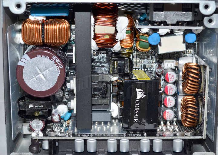
This is my first visit to this site, and the title of this thread caught my attention. Good reading, but I was shocked to find the fundamental part of improving Power Supplies was not touched on at all, namely Power Electronics Topology and efficiency. The first fact about modern power supplies is they are quite grossly inefficient, and are founded on the Buck converter and its derivatives (forward, bridge, etc), including the resonant variants like the LLC resonant converter based on half/full bridge drivers. The Buck converter was invented during the 1950’s and improvements in high frequency switching devices, has largely hidden the failings of this topology. There have been great strides made over 60y but the fact is a lot of waste heat accompanies the power conversion process, and looking at the limiting factors in the process reveals almost without exception, all modern topologies use the air-gapped inductor for energy storage and power transfer. Inserting an air-gap into what is an AC-inductor to convert it to a DC-inductor so it may pass a large DC current, is the root cause of bad efficiency, large size and poor energy transfer capability. The hope of multi-MegaHertz switching to reduce size has been proven futile, as this also brings reduced operating core flux density, increased core losses and increased switching losses, that offset much of the size reductions.
Several problems underpin inductive energy storage topologies, in that currents are hard switched causing noise generation resulting in need for filtering, and various resonant topologies that reduce switching losses have not alleviated the underlying issue of inefficient inductive energy storage. There is much more that could be said on this topic, but suffice it to say 90% efficiency is the norm here, with slightly better efficiency obtained only at the price of greater increased size. But yet new topologies are now available that will allow the Buck converter and its derivatives to be retired - new topologies have already been invented over the course of the last decade. Several new elements have emerged that offer efficiencies in the 98% to 99.5% range which reduces waste heat by over 80%.
First and foremost capacitive energy storage is by far more compact by 2 orders of magnitude, and coupled with a new PWM-resonant switching topology allows single cycle response settling times, and zero current switching, dramatically increases efficiency overall. An inductor and capacitor resonant network is still in play, but introduction of resonance scaling allows capacitance to be increased by 2 orders of magnitude, with a corresponding reduction in the size of the inductor component, and what’s more this is now achievable at 50kHz frequency instead of MHz frequencies; which save considerably on switching losses. Power supply size reduction approaches >80% in eliminating ferrite cores and large heat sinks, with a corresponding cost reduction. For example the inductor has no ferrite core (i.e. air-cored) and becomes a 5 mm length of copper wire, while a bank of ceramic chip capacitors in parallel are minuscule compared to what is used today. These technologies also offer reduced operating flux densities for high frequency isolation transformers, that operate purely as AC transformers with no need for air-gaps to pass DC current.
Here is a link to an article describing some of these new elements.
The ATX PSU operates at 98% efficiency with a single stage PFC and DC-DC converter, generating much less EMI noise than today’s PSU. The motherboard VRM operates at 99% efficiency using just a single stage for each of the CPU, GPU, and memory components, with response settling times an order of magnitude faster than the multi-stage buck converters. The GPU itself also would use a similar VRM.
There is really no reason why memory modules could not incorporate their VRM on each memory module, so small is this new switching topology. The entire VRM is now just a single chip incorporating controller and power stage.

 no
no