Hey all, @Heimdallr here due to popular demand. We throw around many acronyms every day on tech forums without actually having basic knowledge of what these things do. One such acronym you’ll hear amongst us hardware geeks like @MisteryAngel and I are VRMs. It stands for Voltage Regulator Module (VRM) and it is an electronic circuit that regulates and down-converts the voltage from its input from the power supply to the integrated circuits on the motherboard including the CPU etc. Thats a simple task but very essential as the VRM converts the various 12/5/3.3 V DC Power Rail voltages that come from a power supply unit into the lower operating voltages of the integrated circuit (i.e. 0.7 V, 1 V, 1.25 V and sometimes even lower or higher). Now us engineers we like efficiency so these devices are typically implemented with a switching style buck converter which is very efficient compared to other regulation systems.
Let’s get into a largely oversimplified but detailed explanation of the basics. Through this post you will have many terms defined for you that are common use when discussing power delivery on most PC systems. Enjoy!
So let us analyze the simple single phase VRM (not commonplace on today’s PCs for good reason).
Here is a super oversimplified and generalized circuit diagram drawn up in Spice

Now as you should know from reading above this is essentially a buck converter though there’s never just one strict way to design such a converter. On the left side we have a 12 Volt Power supply unit. There are two MOSFETs before Node A. These FETs are distinguished by being on a high side and a low side which serves are actual switches (similar to your light switch through the rate it can switch at is vastly higher). Now, node B is the choke. It’s an inductor that serves as a filter for the ripple of this switching supply. Inductors attempt to maintain constant current by manipulating the voltage and thus the reason for the flyback diode that limits the current on the VRM. The overarching goal of this circuit is to take the PSU voltage from 12 Volts down to the operating voltage of your CPU or GPU. You can see now why changing the voltage and not running at the lowest stable point can put a lot of stress on your VRM system already.
Now when the high side switch closes; the voltage at node A becomes 12 V instantaneously however the voltage at the node B side of the inductor doesn’t change instantaneously. This is due to the fact that the inductor continues to resist changes in current throughout the circuit. As the 12 V is applied to the inductor or choke, the choke builds up a magnetic field which in turn causes a voltage drop at Node B. As the inductor builds a larger magnetic field; You may think of this like a battery charging however the field principles are different; the voltage drop continues to minimize until the field equalizes at 12 V potential. This is what will occur when the high side closes for sufficient time.
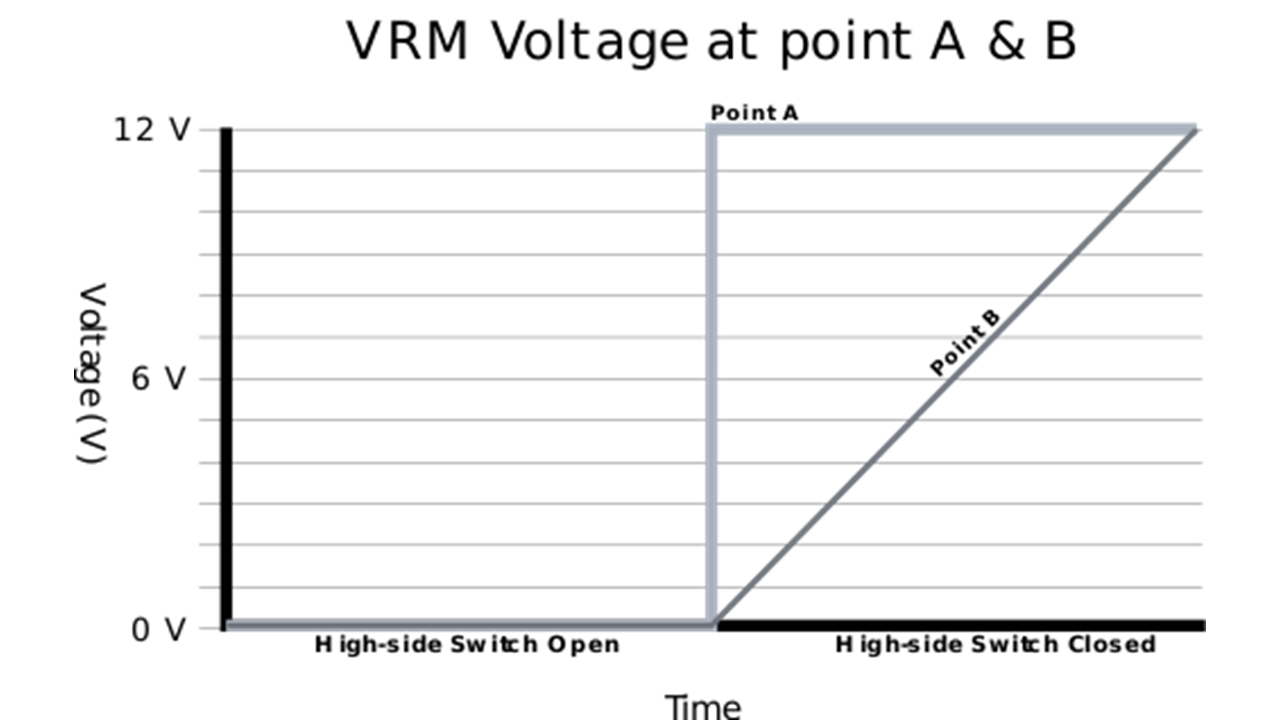
Now the inductor does server as a protection against instantaneous voltage changes which are dangerous to the onboard components. The inductor also determines how fast the circuits can switch via its actual inductance value. This measurement is measured in Henrys (H). To better visualize this a small inductor with a low inductance will change and respond much faster vs the opposite because it builds a smaller field.
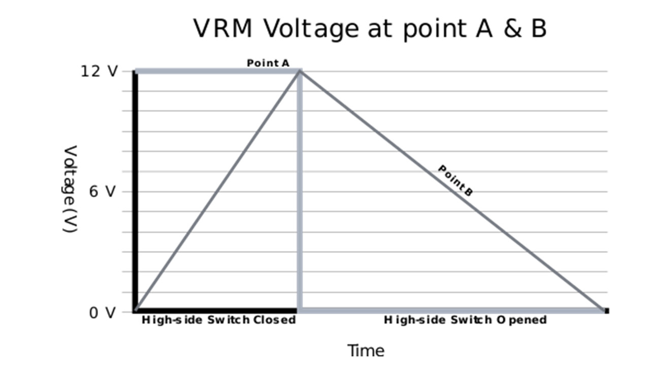
Now when the high side opens again and the low side closes; the voltage at node A drops back to 0 Volts or ground (I say this because technically its never 0 its GND ref). The inductor retains the magnetic field that was built up when we charged it however just like you everything likes to be in an equilibrium state (balanced). Thus the inductor’s magnetic field starts to collapse generating a current at node B which is fed to the CPU since CPUs are current hungry and not voltage hungry devices contrary to popular belief. The problem with this is that at Node B a huge voltage spike occurs so the flyback diode is added to the circuit in order to eliminate this flyback voltage. You don’t want a giant voltage spike to blow your multi-hundred or even multi-thousand dollar CPU to teeny tiny pieces. Shes lost her blue smoke Jim  .
.
Unfortunately, diodes are rather inefficient little semiconductor devices so when the circuit opens the high-side switch it also closes the low-side switch on the circuit. We must do this to allow the current to flow through the switch instead of the diode. The switch/wire is the path of least resistance which increases the efficiency of the overall circuit. Let us take a look at the complete graph of a single period of operation.
We have a pulse and a voltage signal (the triangle) . The measurement of the higher peak to the lower peak is called the ripple voltage magnitude. This is important to consider as too much can hurt your driven circuits.
This entire cycle is repeated forever and ever and ever through a technique known to us geeks and engineers as pulse width modulation. At roughly 50% duty cycle, the output voltage at node B will be 6 Volts! As you can see that’s the average of this rippled wave. Now, let us think about the CPU world. We need to get our desired 1.25 ish V the duty cycle should be about 10-15%. See in our PCs the closing and opening of the low-side and high-side FETs/switches is performed by the PWM Controller coupled with a driver and a lot of times a doubler. let us look at what those two signals overlayed is like.
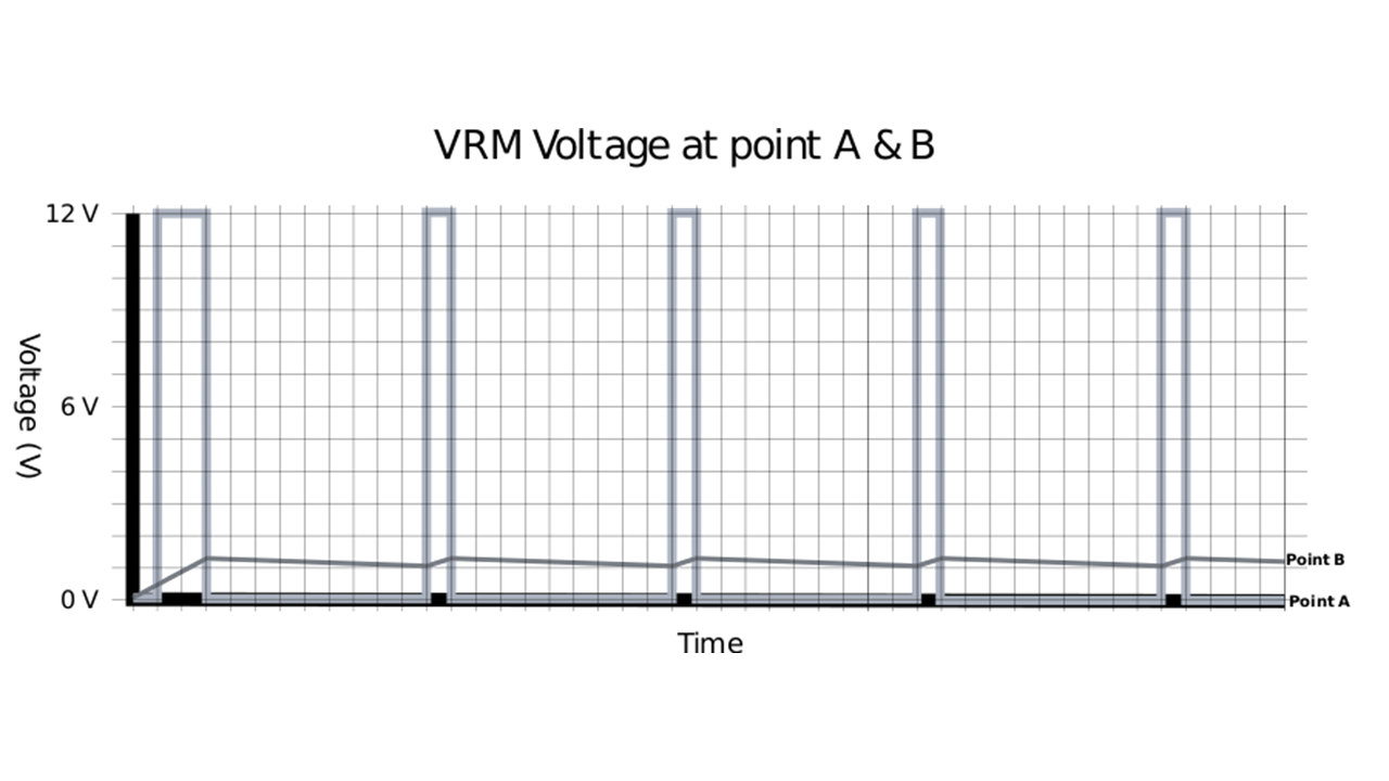
BINGO we got our voltage sure it ripples a bit but no voltage is ever steady not even DC. Pretty cool huh! Don’t worry if you feel lost at this step. I will answer any questions below and if I have made a mistake let me know. I am not infallible. This is a gross oversimplification so that we can understand the basic concept. Unfortunately, it overlooks a lot of other complicated issues in the semiconductor design industry.
Alright alright, I can hear you all now… How the in the flying Mexican spirit animals (No offense meant I think their adorable culture wise) does Multiphase power delivery work. This is where stuff takes a whole multitude of paths and is very much up to the designer but let us look at the basics again.
Drawn horribly in Spice: (FTR I hate spice)
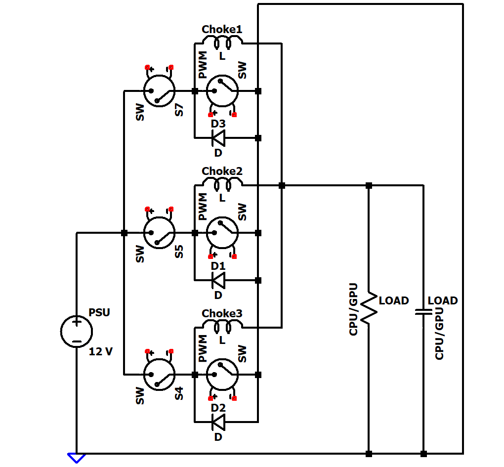
Notice how I labeled the chokes. Each is a different number. In this particular system though NOT labeled … each split off to the high side switches is its own PWM operated phase. This is because the typical motherboard VRM might have 4-6 or more phases. So you see a multi-phase VRM works just like the single-phase VRM described before however its modified to use multiples of such circuits in parallel. This allows each phase to share a small portion or equally divided portion of the load dynamically. The overall idea here is that each of the phases is slightly offset on their PWM signals. This is performed such that at any given time only one phase has the high-side FET switch closed and is building a charge on its inductor. In this mode, the rest of the phases will be discharging their portion of the current to effectively round-robin the current across the phases.

See the top fluctuating signal, that is the voltage that is maintained in this circuit just like the single phase. Normally more phases are more efficient however its not always the case. It’s also worth mentioning that since the total amount of current fed to the CPU remains more or less unchanged from a singular phase VRM that the total current is now distributed among the multiple phases. This allows for much cooler and efficient operation. This also allows more current capacity should it be needed.
Let us take a 2 phase VRM for example, each of the phases will see roughly 50% of the current on average. You can see why this would prolong the devices on the VRM as each is far less stressed.
There is a sort of catch 22:
You see now there is some very much unwanted ripple at the switching node A when using these converters. How can we reduce that voltage ripple? Well, guess what? The more phases, the less the ripple effect is observed because there is a reduction in the ripple magnitude and thus also a reduction in ripple current. This reduction of the ripple increases efficiency!
There are however diminishing returns here on this nice little reduction; That is, going from 2-phases to 4-phases will result in the reduction in ripple current is more than going from 6-phase to 8-phases. This is why the efficiency curve when speaking about 6 and true 8 phase systems is not really worth mentioning. The difference in these systems is not made for efficiency this choice is made for total provided current! This is a careful and expensive design choice. Engineers will opt for doublers and various doubler designs to make up for the loss of a phase.
Well what are doublers, what can they do, why are they sometimes used? whats good and bad?
As we know VRMs are driven by a PWM controller. This controller can come in a variety of phases. Usually 4, 6, or 8 total phases. There are very rare exotic PWMs that go up to 10 but these are not usually used for reasons primarily being cost. Motherboard manufacturers typically offer strangely high numbers of phases through what is called doubling. These are performed through doublers which can allow for 12, 16 and even 24! outstanding power phases on the VRM. The doublers function is to double the number of phases off a signular signal (seen below) by interleaving (half the frequency and offset) the signals that are formed using the original phase. Heres a graphical representaion:
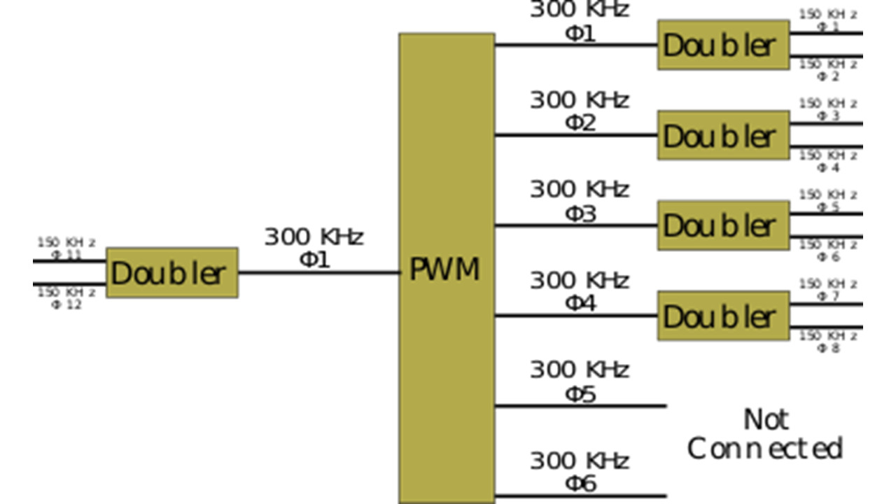
Apologies for the horrible resolution but I hope this presents what I am speaking about better. See how the frequency halves to make two signals which can be interleaved and deinterleaved to make the various signals. We attempt to do this as least often as possible for various engineering reasons that really can’t be described here.
Here is its corresponding output PWM wise… Pretty cool right!
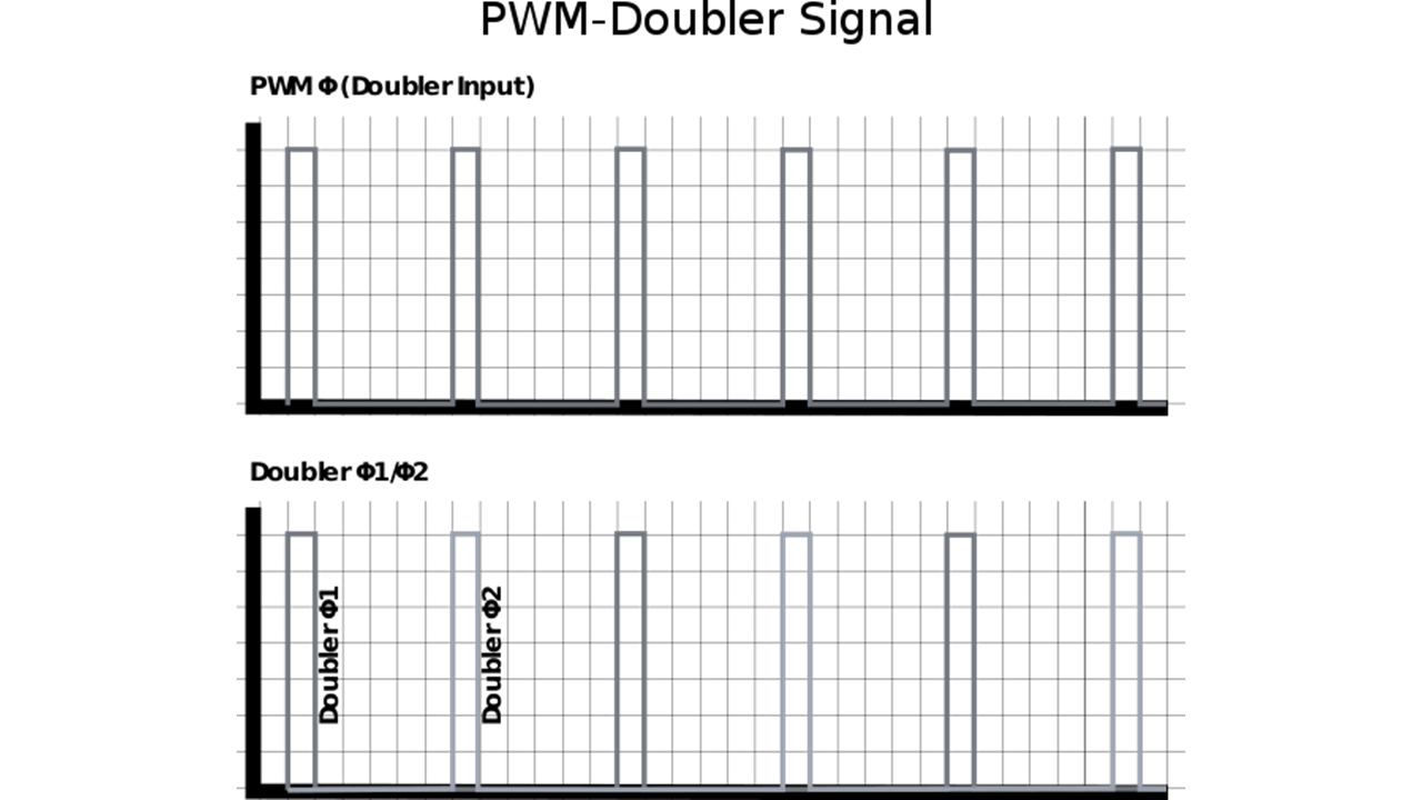
You see the phase output is still going to respond at the same rate (just as fast as true multi phase. Its the voltage tolerance and ability to regulate as tightly that suffers). True phases are true PWM signals controlled by actual phases in the controller. Virtual phases are created by doublers!
Here is a frequently noted issue on the manufacturer and most certainly on the consumer side of the design process. The use of doublers will increase the costs of the motherboard. You now have double the ICs to place on the motherboard.
Now let us clear up a few things about doublers. When implemented properly it reduces many things such as the load current on any given phase in a similar manner to what true hardware multi-phase PWM VRMs would do. Like I said above, this is without the benefits of the tighter voltage tolerances that may be needed for extreme overclocking. It’s also the most common solution found on doubled boards that advertise and boast 8 or even 16 phases.
Now there are poorer implementations. Im going to show one such below:

Once again puked up in spice for your viewing pleasure LOL. This nasty little bugger is a doubler however where you see the initial switch branch off is the same exact phase provided to both virtual phases. This is using a single PWM signal to drive two separate circuits. Now it does not behave as you think. Its horrible for extreme overclocking. However, it’s common cheap because the clocking of the PWM signal is only done by a single phase PWM controller. These controllers are vastly cheaper to buy in bulk. Contrary to most peoples popular belief; the doubling of the VRM circuit here results in more overall power as well as cooler running components and higher efficiency. There’s a drawback; it will not EVER result in better voltage thresholds as true phases will perform in a circuit. This threshold limitation on the capability of the circuit prevents them from being used on high-end boards unless you want to cause a fire as MSI did on the AMD FX boards PHAHA… Depending on the motherboard manufacturer, they may or may not call it two phases although it’s really only a single phase and this is what we like to think is happening with doublers and causes most of the hatred towards them but this isn’t always the implementation so do not judge a board by its DOUBLERS! At least until you have evaluated its actual design.
Now you think this is all fantastic we are cruise control now? No we aren’t! not yet!
REGULATION and FEEDBACK PROCESSES:
The CPU or GPU voltage is never constant due to efficiency design considerations. Thus we must adjust the voltage and frequency using what are called Dynamic Voltage Frequency Shifting Processes or DVFS process/techniques. This will dynamically change the load on the VRM circuit based on how we are using the processor. Now we can kind of treat the VRM like a black box. What’s inside does not matter we already know how it behaves.
The power unit or delivery system controls this feedback system. The unit almost always uses a negative feedback loop in order to correct the voltage levels since positive feedback would rail an amplifier (max out its voltage or destroy it). The feedback method is almost always the same across many different boards. The reference voltage, typically fed from a value inputted into your UEFI/BIOS, is fed into it unit which is then compared with the current monitored voltage. The difference between the Vref and actual voltage fed to the CPU or GPU is used to modify the PWM signal in an attempt to more accurately correct the real voltage signal being sent to the CPU through the VRM. This behavior is performed in real time by a microcontroller. Ultimately you want the desired voltage and fed voltage to match. There are two types of these designs. You have analog (which is fading in recent years) and digital.
Let us start with analog PWM:
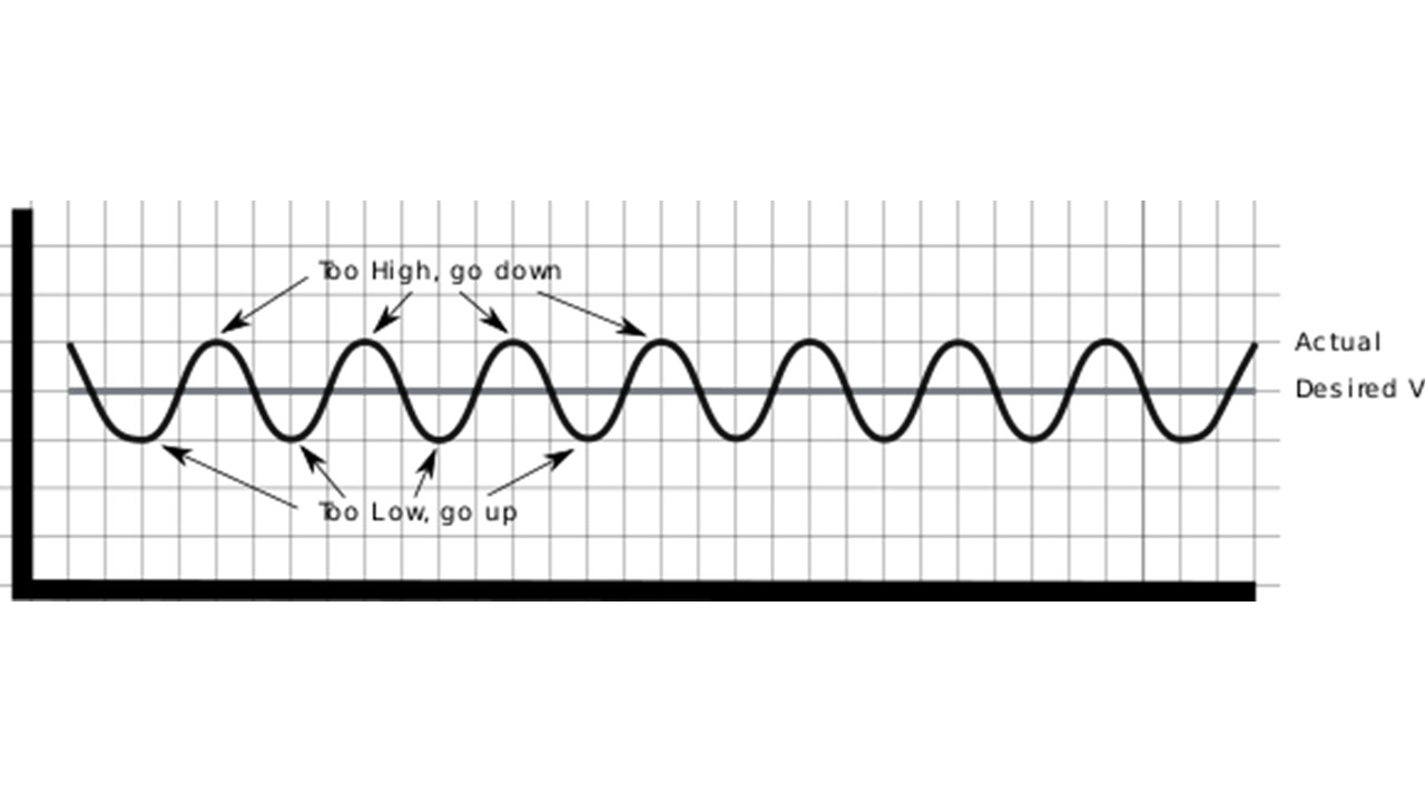
In this representation, the voltage varies in a nearly perfect sinusoidal manner which is generally a constant fluctuation centered about your desired voltage. There are some nice benefits of analog PWM control. If the voltage is too low when compared against the desired voltage, the VRM will compensate for it and shift slightly off from the previous signal. This is performed until the voltage is too high. When we are too high the voltage will start to go down by shifting it slightly lower on each proceeding signal until the voltage is too low. This cycle rinses and repeats and is controlled via a few feedback mechanisms controlled by various circuity I will not get into for simplicities sake. (For engineers you know that this is done via an error op amp with a ramp generator and current balancing mechanism based on current feedback which feeds into the signal gen) Lets stop there for laymans terms.
There are some advantages to this technique! The fact that it’s all done in hardware implementation makes its reaction time and corrections considerably faster than digital which may or may not be the case anymore! It’s also cheaper, easier to implement in a correct way since its tried and tested technology.
Below is an intersil ISL 6366 6+1 Phase Analog PWM controller!
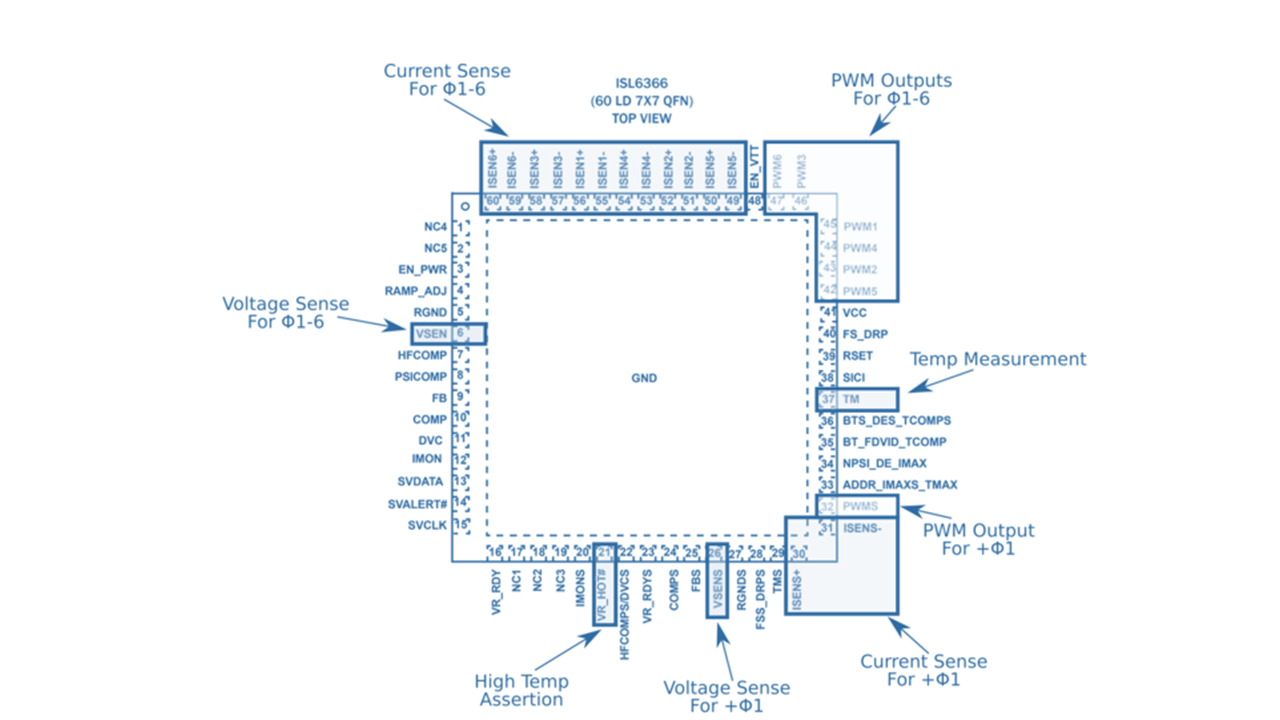
Check her out! Decent amount of phases pretty simple controller if I do say so myself! Feel free to examine it! I can explain and answer further questions below
DIGITAL PWM:
This is our modern implementation on most boards!
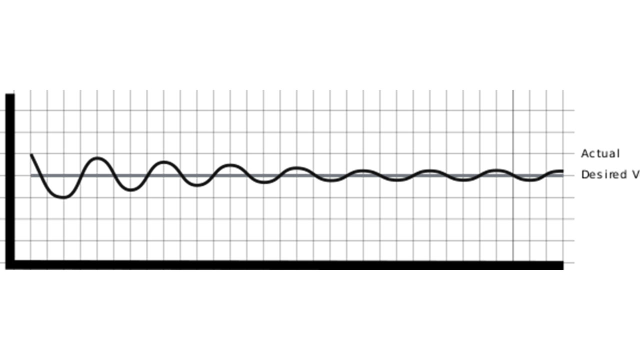

As can be seen, a digital PWM circuit has the reference voltage digitally fed to the controller. However, all the feedback values and monitoring is fed through an analog to digital converter which quantizes (creates a digital number) into bits for digital representation and computation in a microcontroller. These microcontrollers settings are fed from your UEFI or BIOS on some extreme overclocking boards even finer control of this controller is permitted. this is a basic design above. These get so much more complicated and proprietary amongst the various vendors. These circuits can take into account so many more variables and are controlled by a control mechanism known as PID (proportional integral derivative) control. Without going into more detail here (I will of course elaborate below)… this will take all the values in and determine exactly how high and low to go and attempt to minimize the over and undershoot to nearly zero as can be seen in the graph. this is how your speedometer works in your car as well!
These designs have a lot of issues unbeknownst to the user. They are expensive. they are fairly complex to code for. The algorithms are extremely complex in order to be so accurate. These devices are never perfect because the sampling rates are still too slow so dithering must be applied (see Wikipedia article)!
What the heck does 6+1 or 8+1+1 mean?
In addition to the CPU or GPU cores there are many other voltages on your motherboard which include but are not limited to:
- CPU Voltage (VCORE)
- System voltages such as VccSA
- QPI/VTT Voltages
- IMC Voltage
- DRAM Voltages
- SOC Voltage
Engineers and marketers needed a standard way to indicate how this hardware was being used. This did not exactly come to a standard through most OEMs will indicate it using the “A+B” or “A+B+C” notation on the specifications page. The “+B” and “+C” are normally used to indicate that those phases are being used for different voltage rails discussed above and are often shared amongst many common voltage lower current devices! Let us examine a common notation: “6+2” will more often than not indicate that 6 of the phases can be used together for one of the voltage rails. This voltage rail is ALMOST ALWAYS the CPU or GPU (depending on whether its the motherboard or graphics card). The other 2 phases can be used for remaining rails. In some cases, not all phases are used. Some are permanently disabled or optimized to be on during certain conditions are simply not connected. The not connected case usually occurs in same manufacturer different SKU common platform designs where buying different parts does not make economic sense. It must be noted that other PWM controllers may and should be added for the other rails not common to a CPU or GPU. Also it should notated that for most PWM controlled VRMS the voltage rails cannot be combined. A 6+2 can never be an 8 phase controller for only the CPU power.
This concludes a simplified however detailed explanation of Power Delivery on the motherboards!
Questions and suggestions accepted!
Heres a graphics card layout detailed on EVGA forums.
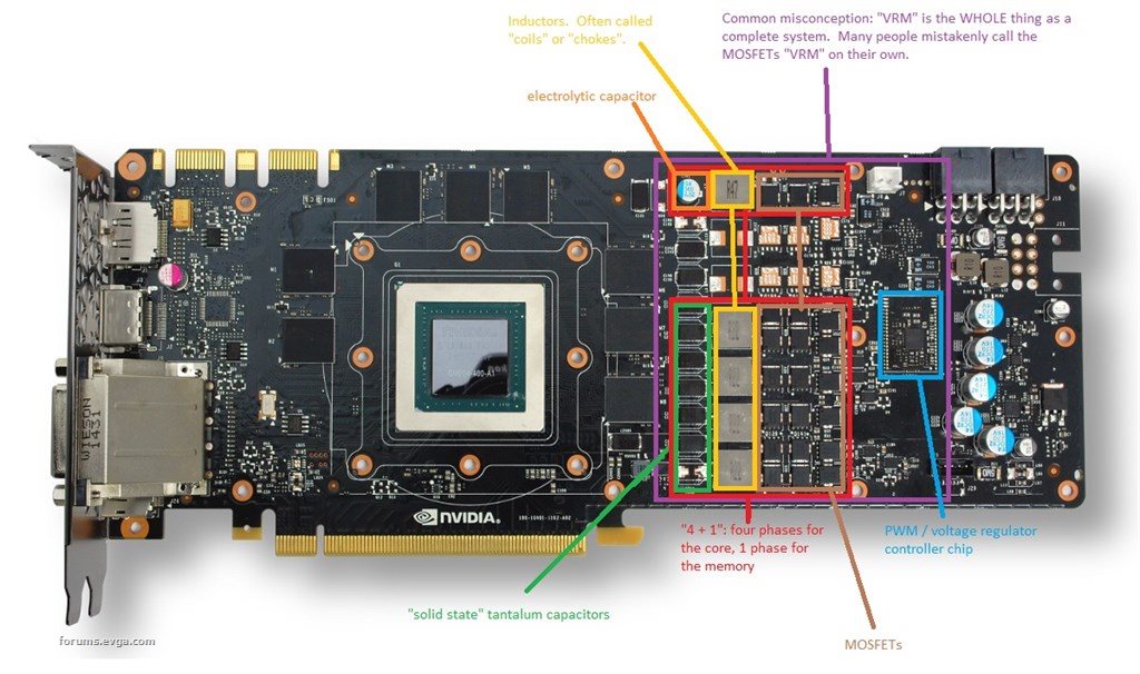
Its a GTX 980 before anybody starts arguing over what it is LOL.
If anyone has a well detailed/labeled motherboard picture I will take it!
Expansion can and will occur and this post may possibly be wiki’d so I can pawn some of that work off on helpful people in the forum! haha
Glossary (Added per demand):
MOSFET- A MOSFET (metal-oxide semiconductor field-effect transistor) is a specialized FET (field-effect transistor), and like all transistors, is used for switching or amplifying signals. MOSFETs are now even more common than BJTs (bipolar junction transistors) in digital and analog circuits. (WIKIPEDIA)
**DITHERING – ** the process of adding white noise to a digital signal to reduce distortion of the low-amplitude signals and/or primary harmonics (SEE WIKIPEDIA FOR MORE INFO)