I keep seeing similar looking roadmap charts with minor changes between them, so I thought I would make a post here with what I find as most recent info:
POWER9 SO
POWER9 SU
POWER9’
POWER10
General Availability
2017
2018
2019
2021+
Cores
12/24
12/24
12/24
TBA
Lithography
Globalfoundries 14nm
Globalfoundries 14nm
Globalfoundries 14nm
Samsung 7nm
Marketing
New Micro-Architecture
Direct Attach Memory
New Process Technology
Enhanced Micro-Architecture
Buffered Memory
Enhanced Micro-Architecture
New Memory Subsystem
New Micro-Architecture
New Technology
Sustained memory bandwidth
150 GB/s
210 GB/s
400 GB/s
435+ GB/s
Standard I/O Interconnect
PCIe Gen4 x48
PCIe Gen4 x48
PCIe Gen4 x48
PCIe Gen5
Advanced I/O Signaling
25 GT/s 300 GB/s
25 GT/s 300 GB/s
25 GT/s 300 GB/s
32 & 50 GT/s
Advanced I/O Architecture
CAPI 2.0, OpenCAPI 3.0, NVLink 2.0
CAPI 2.0, OpenCAPI 3.0, NVLink 2.0
CAPI 2.0, OpenCAPI 4.0, NVLink 3.0
TBA
I’m mainly using the 2018 October EU OpenPOWER Summit OpenCAPI presentation as a reference, but also adding info from a Jeff Stuechelli video saying 400 GB/s per socket, and POWER10 as “some time after 2020”.
IBM terminology
The suffixes used for revisions of POWER chips have specific meanings:
Plus sign +
a “plus” chip in the IBM lingo means something very precise, and that is usually a process shrink coupled with some slight microarchitecture changes
from NextPlatform article on new roadmap (April 2016)
Prime symbol ’
it designates a change in the I/O and possibly memory subsystems in a Power processor; it is distinct from a plus sign, which means a change in process or architecture or both in a Power chip, but well short of a major version which has big changes
from Nextplatform article on Samsung as POWER10 fab (December 2018)
Hmm… I wonder if that POWER9’ chip coming out this year in 2019 will be drop in compatible with existing boards? Am I reading your chart correctly @olddellian?
I am almost certain that no, it will not be. The main point of buying one of these would be to use OpenCAPI 4.0 or NVLink 3.0, which would probably need a board redesign anyway.
NextPlatform wrote last year about POWER9’ potentially using OpenCAPI to interface with OpenCAPI memory as an alternative to POWER9 SU using SerDes to talk with Centaur-buffered memory; this is potentially further incompatibility with POWER9 SO&SU boards. You can read about OpenCAPI memory here: https://www.nextplatform.com/2018/08/28/ibm-power-chips-blur-the-lines-to-memory-and-accelerators/
I’ve done a bit of skimming through the skiboot repo (details are collapsed below) but I’ve come across some interesting observations.
POWER8E is separate from POWER8 NVLink (wiki needs to be updated I guess)
multiple places in the code order POWER8E before POWER8
this newer “POWER9P” chip has a codename “Axone”; this is probably to stress IBM’s new PowerAXON naming for the combined A Bus, X Bus, OpenCAPI, and NVLink interface
while POWER7+ is shortened to P7P in places, I still don’t think P9P is meant to imply POWER9+. cpu-common.c for example treats P9P as just another POWER9 chip, while P7P (POWER7+) is treated as an entirely separate chip from P7
Chip Lists from Specific Files
doc/platforms-and-cpus.rst
Power8E   0x004bxxxx Murano
Power8    0x004dxxxx Venice
Power8NVL 0x004cxxxx Naples
Power9N   0x004e0xxx Nimbus 12 small core
Power9N   0x004e1xxx Nimbus 24 small core
Power9C   0x004e2xxx Cumulus 12 small core
Power9C   0x004e3xxx Cumulus 24 small core
Power9P   0x004fxxxx Axone
Axone being optionally 12c or 24c, though if it’s a minor modification from Cumulus/Nimbus, I can’t image it not sharing the same properties
It is interesting that the skiboot code/documentation groups SMT4 and SMT8 together like this, I assume this means that SMT4 vs SMT8 really is just the same silicon. I wonder if it is possible to turn a SMT4 chip into SMT8 or vice versa…
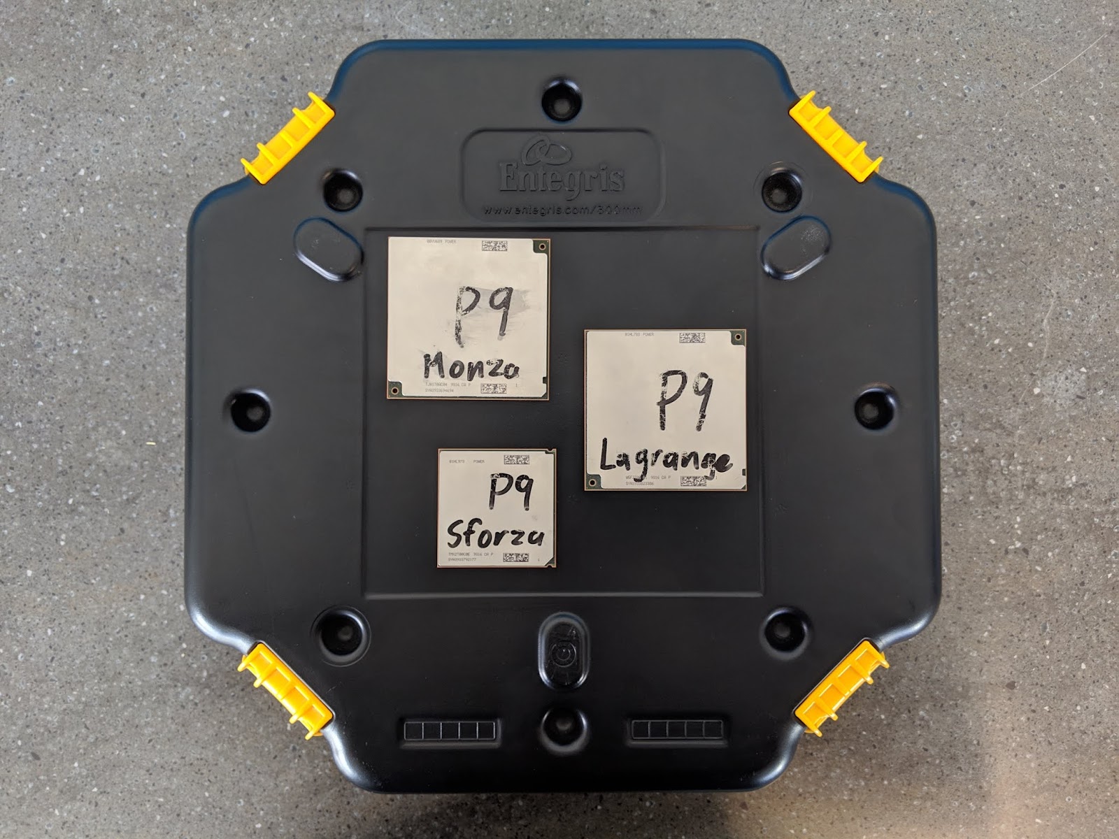
Looks like that single socket LaGrange mainboard they mentioned on Twitter last year is coming along nicely; they mentioned it unprompted in a recent tweet:
Apparently earlier this year, Wikipedia editors decided to restructure a bunch of the Power-related articles to remove references to “Power Architecture”:
I’m not sure what to make of that, is it really so different from how we refer to x86-64 and x86 (or more precisely, “IA-32”) as x86, or all the different variantions of ARM as ARM architecture?
Personally I’m just annoyed that all the specsheets for tme ppc machines are wrong on the site. Some of the models are mixed up, a lot of the listed processors are wrong or missing, entire versions of machines gone, no mention of the cost and price difference of the emac and how they had sold 3 versions of the same machine at the same time…
the OzLabs developers like the T2 so much they’re ordering more as workstations
He mentions the mapping between some prototype names and the final products they became:
Romulus → Talos II
Witherspoon → AC922
Palmetto → Tyan GN70-BP010
Stratton → S821LC
Briggs → S822
And we finally have a picture of all three modules next to each other: