That’s ok, but cpu bound soft-realtime server software (most internet service companies running big clusters of machines) can run at higher utilizations with more parallelism availability. That’s because soft-realtime implies you’re always leaving cores starved so you can target your tail latency limit, the more cores you have to be able to bounce your workload around, the less you have to keep starved/unutilized.
By all means, stick many of these bigger chiplets in one socket and let them communicate with the outside world through old tech, but these single digit threads/request apps are old news in server software.
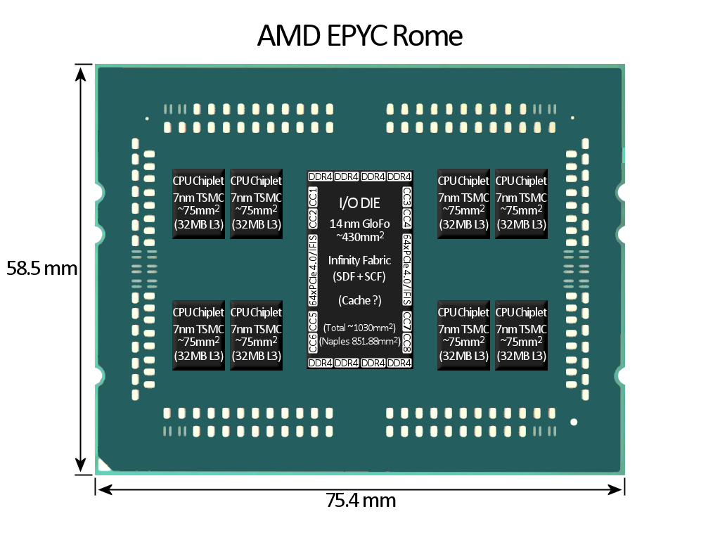
The chiplets are all of the processor core logic. It’s the important bit that does all the hard stuff, the associated SRAM that the cores need to operate efficiently, and PCI-E. The I/O die is exactly that; I/O. It’s kinda like what the northbridge used to be, but very close proximity and significantly higher throughput.
By making chiplets AMD is able to reduce all the densest logic down to 7nm and utilize all the advantages that entails while also leaving out all the parts that generally do not scale down with each process shift, such as the DDR PHYs, serial hosts, infinity fabric interconnects, etc.
Similar to how the MCH/ICH weren’t included in figuring die size during the P4/Core 2 era of Intel parts, the I/O die wouldn’t be counted for Zen2.
There is literally every reason for chiplets to be that tiny, as explained above. More chips per wafer, less defective silicon, better binning. With the lack of the I/O logic they can afford to make them that small.
Also you’re assuming “empty” space on the package. That entire package is filled with layers of interconnects and vias, I’d like to see your brilliant design plan for such a complex MCM.