I have a cheapo NES on a chip (i think) based handheld, it has a flash chip where the magic is stored and i’d like to dump it to analyse whats actually running on this thing, and maybe inject my own stuff.
I’ve found some code on github and a pinout for using something called a 360-clip (possibly for console modding) to interface with a pi to poke at the data on it. The 360 clip doesn’t look to have any active/passive components on it, it looks as if its literally just a breakout cable.
I’ve “hand flashed” bioses on laptops with a rpi and jump wires, this is probably going to be somewhat more difficult due to the finer pitch, but i still think its possible.
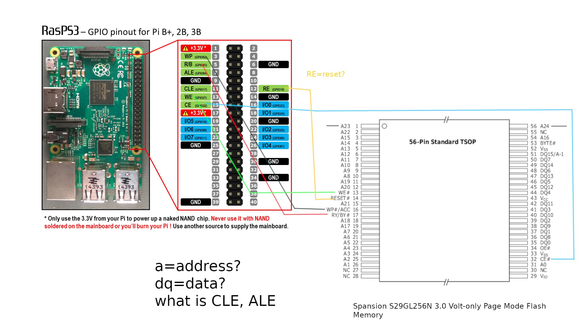
I just need help sorting out the pinout. I’m not sure what ALE, CLE are. DQ is the i/O. Eliminating address/data lines and matching references, i’m left with vcc/vss/nc (known), VIO,OE#, CE#, and BYTE#
hmmm you are right about being able to go to 8 bit address mode, I should have read the datasheet.
8 address + 8 data + 5/6 ancillary pins is less than the 26gpio you have so it would be theoretically possible… however I would be a little worried about the raspberry pi driving the voltage levels “correctly” at speed.
Also I took a quick peek at the code and it looks like it is for accessing serial nand rather than parallel.
Yeah, flash chips in laptops are frequently using 1.8v now intead of 3.3v - i’ve got a bench supply, and as they say “I aInT sKeErD” of rigging that sort of shenanigans up.
I think i need to take a second look at the actual target.
i’ve got a couple of these cheapo handhelds, this is the crappier of the two, i think the other is a tsop48 on a castellated breakout board - i guess for easier manufacturing.
I was gonna do a practice run on the crappier one and then go for the nicer one.
The nicer one has gotten a bit of hype on youtube and such lately because it was going for $10 at five below and had actual NES games on it (probably sans license) . the crappier one had some branding for data east on it, like 5 of their games and the rest are mostly garbage - but it feels cheaper, uses aaa’s instead of a rechargeable lipo like the one from five below.
I figure if i can get the flash chip dumped and run it through binwalk to sort out if it looks like 6502 code i might be able to map out the file and inject my own roms in there.
speaking of the one from five below, the fact they were selling for $10, with the old nokia battery, samsung flash chip, and LCD i’m curious as to how the hell they were making money selling them for $10.
Hey, if the flash chip is indeed 1.8V logic, you may be able to use resistor dividers for the IO pins. I used this for a similar problem where I wanted to control a 5V logic display from a 3.3V MCU.
If the flash chip outputs a voltage higher than the logical-high threshold of the RPi GPIO, you should be able to read the data.
Of course, this isn’t garanteed to be fast or reliable, but if all you need is to dump out the ROM contents, you should be able to find a clockrate that works.
If we’re talking S29GL256N, it’s definitely 3.3v, but in order to read/write at speed its usually necessary to overdrive the pins alittle bit with perhaps 400mV more in order to be reliable… alternatively you could just not read/write so fast.