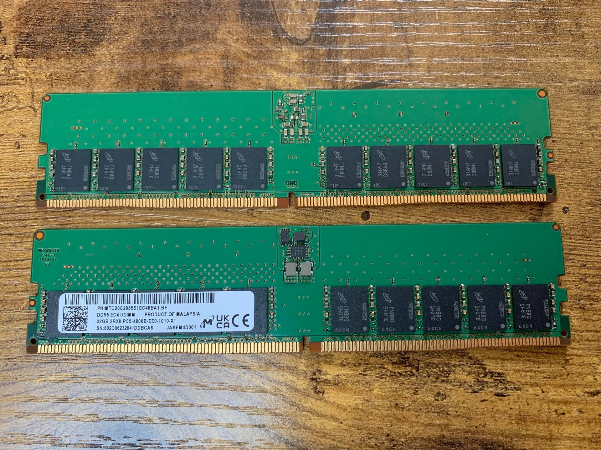
None, if it’s an EC4 UDIMM and an EC4 RDIMM (x72). If it’s an EC8 (x80) RDIMM chipkill can be handled instead of just SECDED.
For EC4 UDIMMs, yes. The on-die EC2’s only SEC. However, since DDR5 has write CRC, read CRC, and EC2 scrubbing, SECDED is semi-redundant.
You’ve discovered why UDIMMs and RDIMMs aren’t pin compatible in DDR5. CB[3:0]_A and CB[3:0]_B are the two subchannels’ EC4s. On an RDIMM these expand to CB[7:0]_A and CB[7:0]_B (Table 4) but on EC4 (x72) RDIMMs I believe only 3:0 are used.
That might be it. If UDIMMs are always EC4 and RDIMMs are always EC8, and these modules were early and had some vestigial bits from an inadequate supply of special-purpose chips, or, something… there’s no contradiction then.
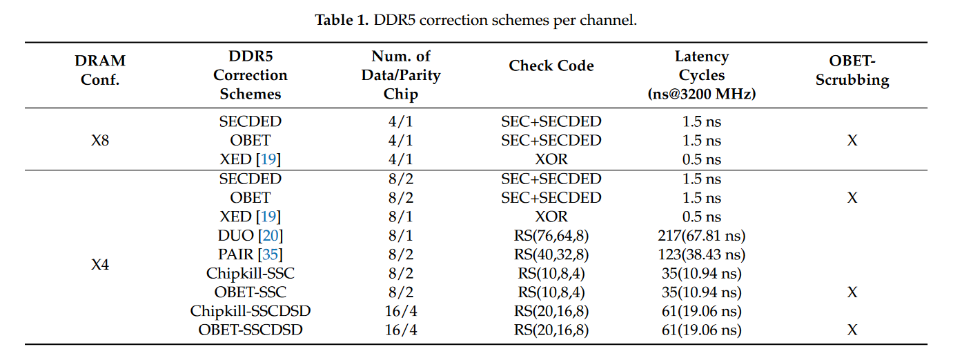
Yeah you’re right, there should have been a 8/1 entry within the x8 DRAM configuration to account for the UDIMMs; this chart is only useful for EC4 and EC8 RDIMMs. I don’t think I’ve ever seen or heard of x4 configured UDIMMs before.
There are definitely EC4 DDR5 RDIMMs in the wild. In addition the ECC ability of different DDR5 RDIMMs wildly varies depending on DRAM chip width configuration and rank.
Wendell calls out the same reported width difference in that first video he linked in this thread, with Micron DIMMs reporting 80 bits. Here’s a link with the timestamp, if you’re curious: https://www.youtube.com/watch?v=RdYToqy05pI&t=730s
Looks like it’s Table 1 of Nguyen et al. 2021 who, at a glance, seem concerned solely with improvements beyond DDR5 on-die ECC. I’ll have to read it later (other things going on, ATM) but, if someone feels like taking a closer look in the meantime, wanted to mention the organizations might therefore not translate well to data bus ECC as currently implemented.
From what I’ve been tease out from some googling around (JEDEC can have their paywall or I can buy RAM, but not both) the ODEC2 (on-die EC2) is 128+8 bit Hamming. Bus EC4 looks like probably at least the 64+8 you suggested with 128+16, 256+32, or 512+64 permitting more correction possibilities.
(edit: revisions from further checking as mentioned in the original)
I watched your videos @wendell. Few things are still not clear to me, but I must also admit that I am no expert in this field. My summary, and please correct me if I am wrong, this is just a layman assumption based on what I read and watched so far:
AM5 and ECC was sketchy at first, but got a lot better now
when buying a system, check with dmidecode if ECC is actually working
no hardware test, but you injected errors with rasdeamon
New questions that came up for me after that:
Is it still necessary to get a Epic or Pro CPU to get ECC? AsRock B650D4U says nothing about that in the QVL or manual, but supports something like a Ryzen 7700 or a none Pro 8300G. So in theory that could work, but at the same time did AMD deleted form reddit that the 8300G supports ECC. AMD confirms Ryzen 8000G APUs don't support ECC RAM, despite initial claims | Tom's Hardware
To me this looks like the typical AMD mess.
Is inserting a double error in rasdeamon trustworthy? Maybe if you could explain in a video how that actually works or what actually happens when you do this, this could build trust in the process. Someone like me, who does not understand the process is a little bit skeptical and would rather like to see a hardware test like with DDR4.
no hardware test, but you injected errors with rasdeamon
Yes, hardware test! Hardware test is even running the memory beyond spec to generate errors, doing rowhammer tests, etc. This is the “basic” testing. Advanced testing is rasdaemon.
With the new agesa these are very much hardware tests and very much working.
Is it still necessary to get a Epic or Pro CPU to get ECC?
No. What I was saying in the video was that “end to end” ECC (full rasdaemon support) showed up in consumer boards BEFORE specifically the B650D4U which I thought was odd.
or a none Pro 8300G
This is something else; non-pro APUs don’t get ECC enablement for whatever reason, but this explicitly shows in the tooling. (It might have been the case in the past that 1 bit errors were being silently corrected, but I don’t see how that would be the case on APUs… perhaps older AM5 cpus
Is inserting a double error in rasdeamon trustworthy?
Yes, so the whole world of DDR5 ecc is far more insane than I think you might realize. Most RDImms in the field are 80 bits for example. Lot of x4 and x8 ranks “in hardware” support things like row remapping? Which is only juist now getting platform enablement “in general” vs "ODM specific (read as: dell/hp/lenovo/quanta/etc specific). DDR5 ecc taken full tilt is really something special.
Ecc udimm on am5 is still not quite as special though.
The “hardware test” is easy – overclock the memory till you get errors. But imho this isn’t as sane as just using rasdaemon to check the plumbing end to end.
Thank you wendell for taking the time and answering me!
That is such interesting information.
My outdated DDR4 knowledge was that you can’t really test ECC, because it would take months or even years for some error to show up. I did not know that you can provoke en error simply by running them out of spec and stress them with rowhammer.
Thinking a bit more about this, concatenating transfers for wider codewords like this seems dangerous: any errors affecting multiple transfers (stuck bits etc) would become multi-bit errors in the codeword.
I’m really curious to see the linux kernel EDAC output from someone running DDR5 ECC UDIMMs. Both the number of syndromes reported (should correspond to the number of check bits used in the ECC calculation or maybe not, still don’t think I understand this) and what kind of error correction mode the memory controller claims:
It predates the Zen architecture, but it says this about ECC:
The DRAM error correcting code features an ECC word formed by a symbol based code. The x4 code uses thirty-six 4-bit symbols to make a 144-bit ECC word made up of 128 data bits and 16 check bits.
The x4 code is a single symbol correcting (SSC) and a double symbol detecting (DSD) code. This means the x4 code is able to correct 100% of single symbol errors (any bit error combination within one symbol), and detect 100% of double symbol errors (any bit error combination within two symbols).
(Using Reed-Solomon codes maybe?) So it corrects up to 4 bit-errors if they are all within the same 4-bit symbol? I guess this is where the dmidecode-reported “Multi-bit ECC” comes from?
Later:
The error address maps to the two DIMMs composing the 128-bit line
Hmm, so what is done in a system with a single DIMM? And what if the DIMMs are on different channels, working on unrelated lines? (Or different subchannels as applied to DDR5? A 144-bit codeword made up of four transfers from the same DIMM with, say, a single stuck column, would be both uncorrectable and undetectable with this technique?) The questions just keep coming!
It also distinguishes between error simulation and DRAM error injection, where the latter intends to “cause a discrepancy between the stored data and the stored ECC value.” It goes on:
Therefore, DRAM error injection is only possible on DRAM which supports ECC.
It’s in Table 67 of the 19h processor programming reference as well (for whatever reason I’m getting no 1Ah hits).
WriteDataPoisonErr. Read-write. Reset: 0. Data poison error. The system tried to write poison data to DRAM and either DRAM does not support ECC or UMC_CH.EccCtrl.WrEccEn is cleared.
L1, L2, L3, and PCIe ECC’s also poisonable. I’d expect to see the same for GDDR in RDNA documentation, though ECC GDDR6 starts with the W7700.
DDR4 and 5 ECC’s multi-transfer, I think, though perhaps not for UDIMMs. AMD appears cryptic for processors but the AMDC tech note suggests a 512+64 code for EC4 DDR4 RDIMMs. Subsequent documentation indicates AMDC remains available for EC4 DDR5, though probably superseded by bounded fault EC4 and EC8. I’m not having luck tying that back to Ryzen via EPYC 4004, though as a default I’d expect an EC4 block reused across IO dies. In AMD’s FPGA portfolio extended Hamming/Hsiao’s common at narrower widths.
AMDC and the bounded fault implementations seem likely Reed-Solomon, which enables 32-64 bit correction and appears minimally necessary to EC8 chipkill support. Criss et al. 2020 offer context on bounding, of which I think your stuck bit concern’s a subset. Hamburg et al.'s preprint may also be of interest, notably the remark about beyond bound correction in Skylake, but more for discussion of optimizing decoding across two transfers, motivations for lockstep, and comparison to other large codeword approaches.