This is a project I’ve been working on for a few weeks now, may as well make it a #devember2020 thing to get the last major details worked out.
About me:
I’m an Australian Computer Science student with my final year next year. I have a particular interest in computer hardware and low level programming (Anything higher level than C confuses me). I’ve also been meaning to improve my electronics skills so why not combine all of these things and make my own computer. How hard can it be!
About the project:
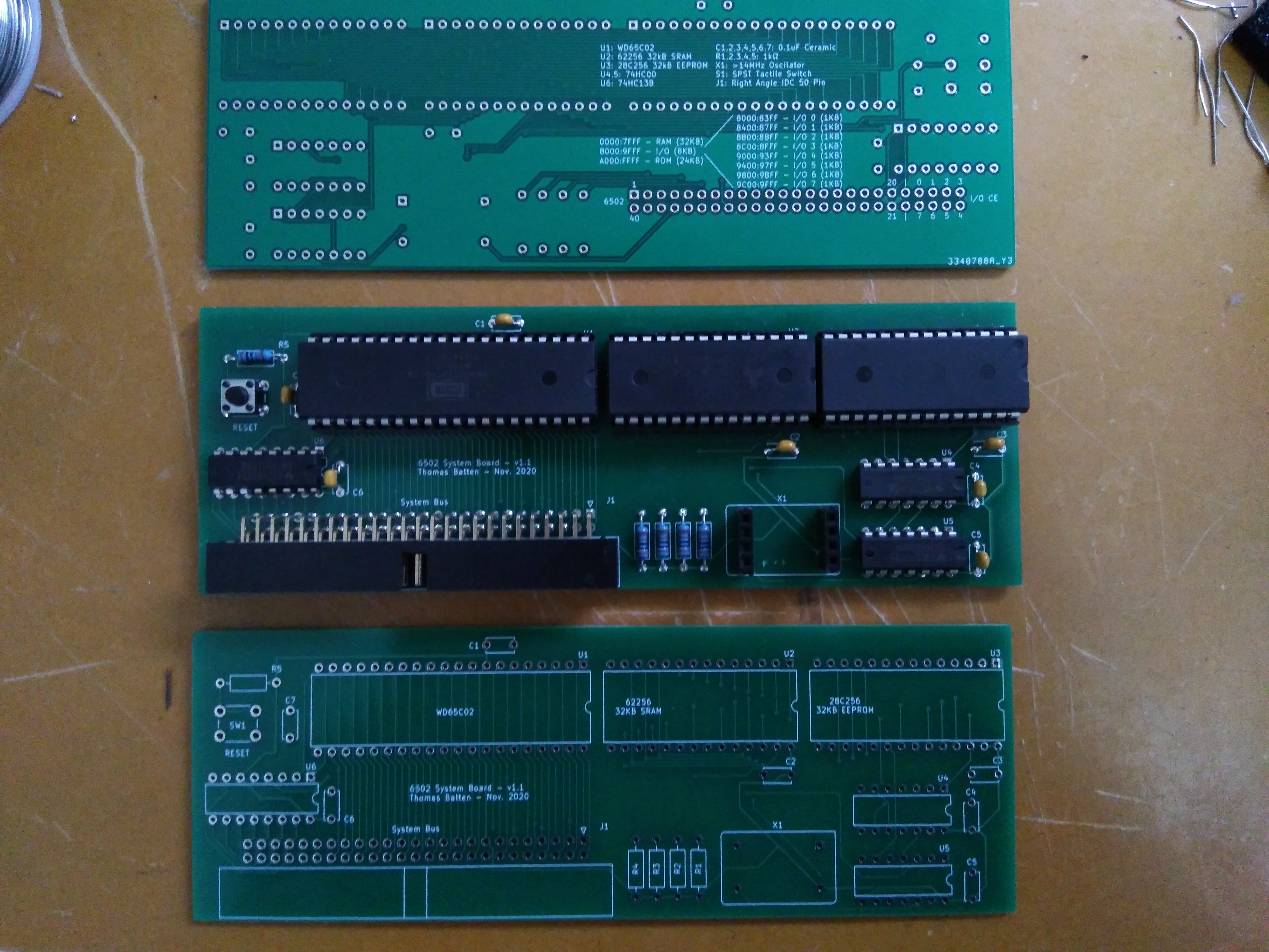
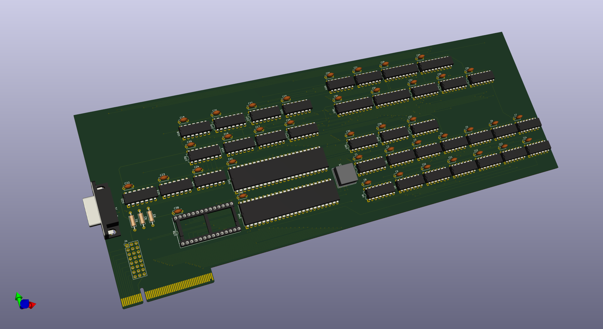
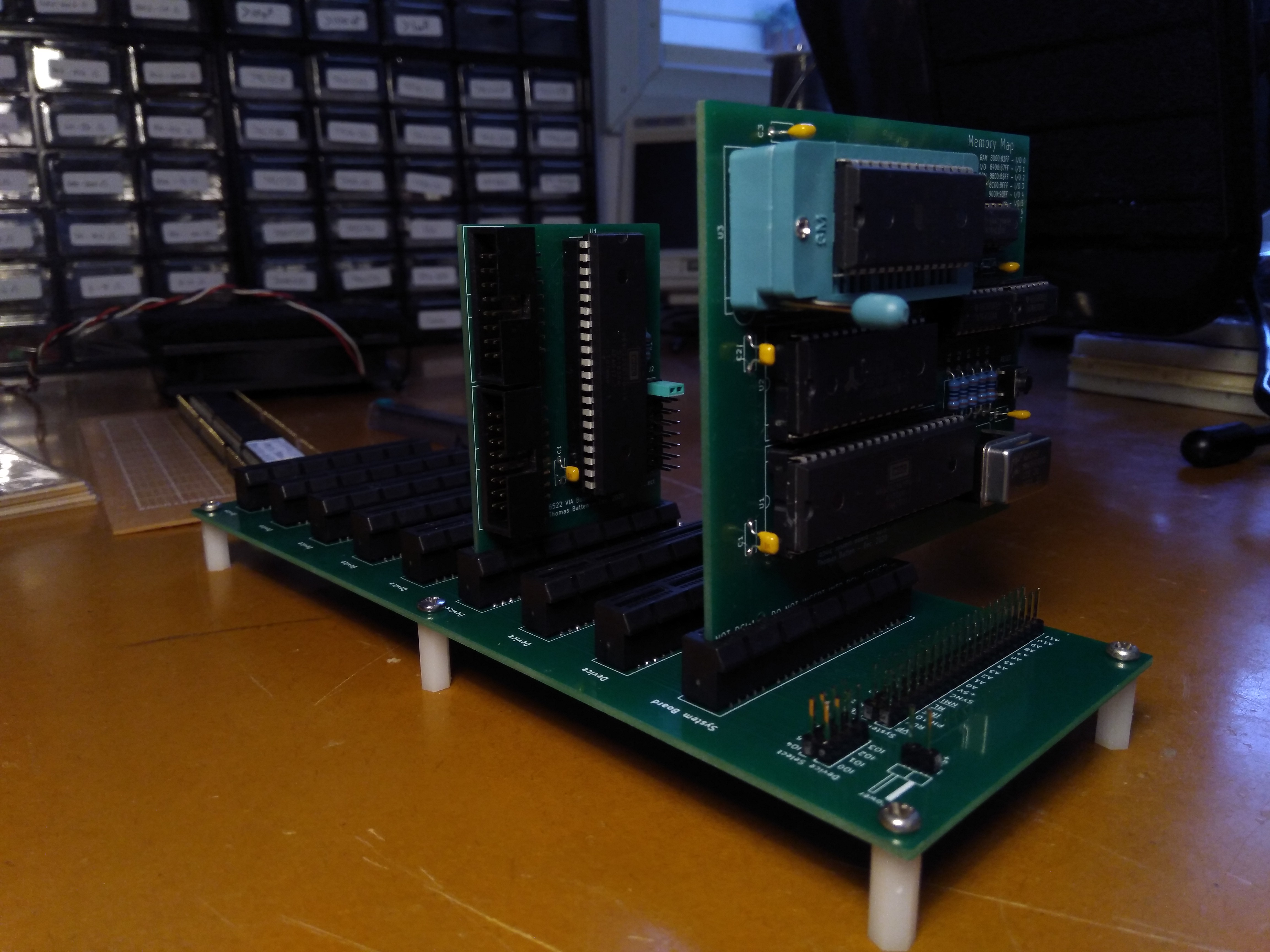
At the core, this is a basic 6502 based computer using all brand new parts (Yes, you can still get 6502’s brand new!) with the ability to add external devices. The computer has 32kB of RAM, 24kB of ROM and 8kB of IO space for up to 8 cards. The devices I’m currently planning are a Serial IO card, Parallel IO card and a VGA text mode display card. This is all heavily inspired by Ben Eater’s YouTube videos but I’m giving it all my own spin and I’m going to get some actual circuit boards made. I actually just today received my first prototype PCB’s and assembled the main computer module:
The parallel card has already been designed and got the PCB for it with the CPU boards. The card I’m currently working on is the VGA card. It will (hopefully) be able to output either 40x25 or 80x25 Text characters at 640x480 which needs only 1kB or 2kB of RAM which is perfect as a single device can access 1kB of address space and I can make a device use as many device slots as I want!
I’m going to make the schematics freely available as I thing other people might like to take a look at this. I’ll post some more details in my next post. Hope you all find this interesting!
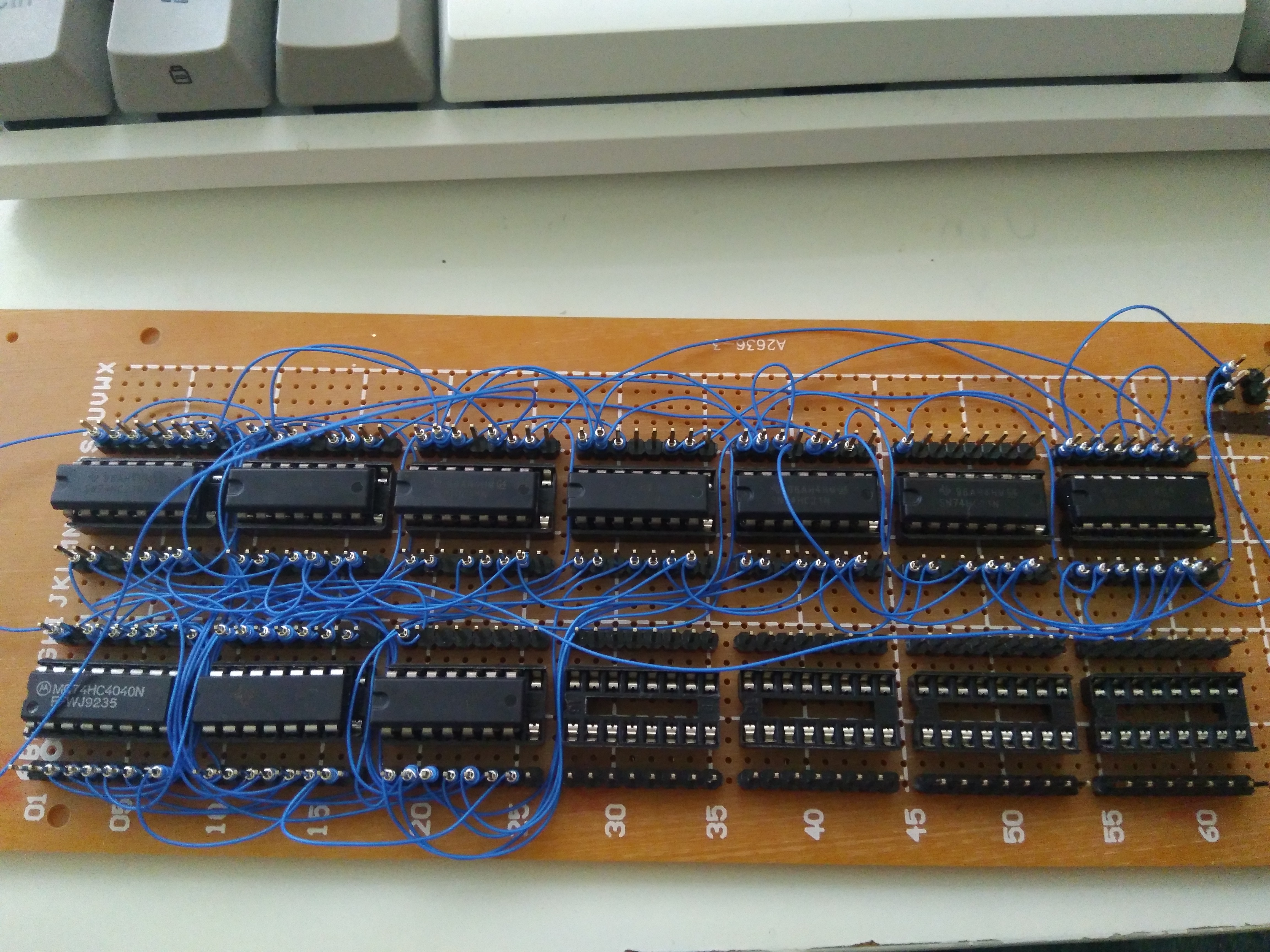
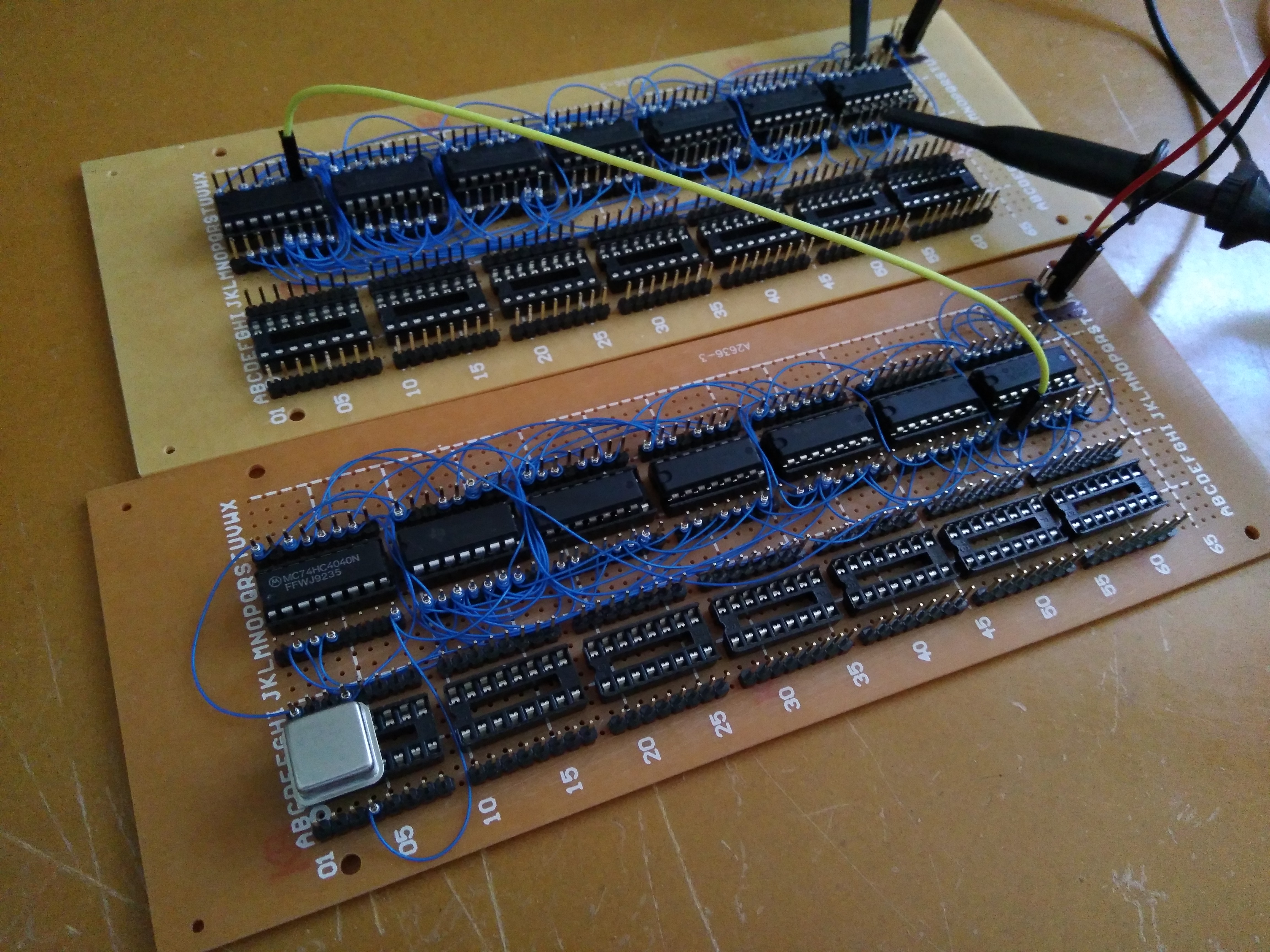
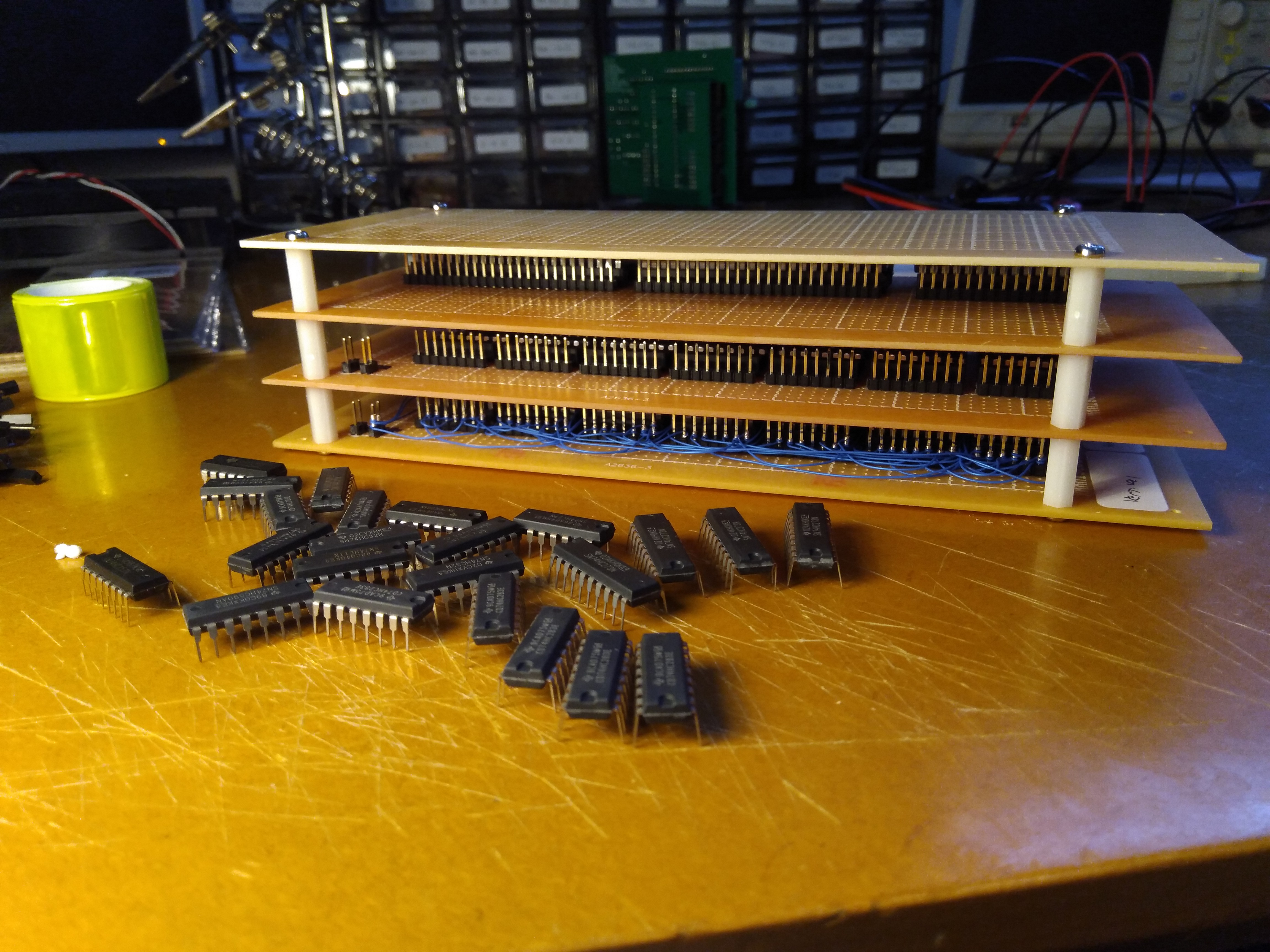
Worked on the VGA card today, tried my hand at wire wrapping for this prototype.
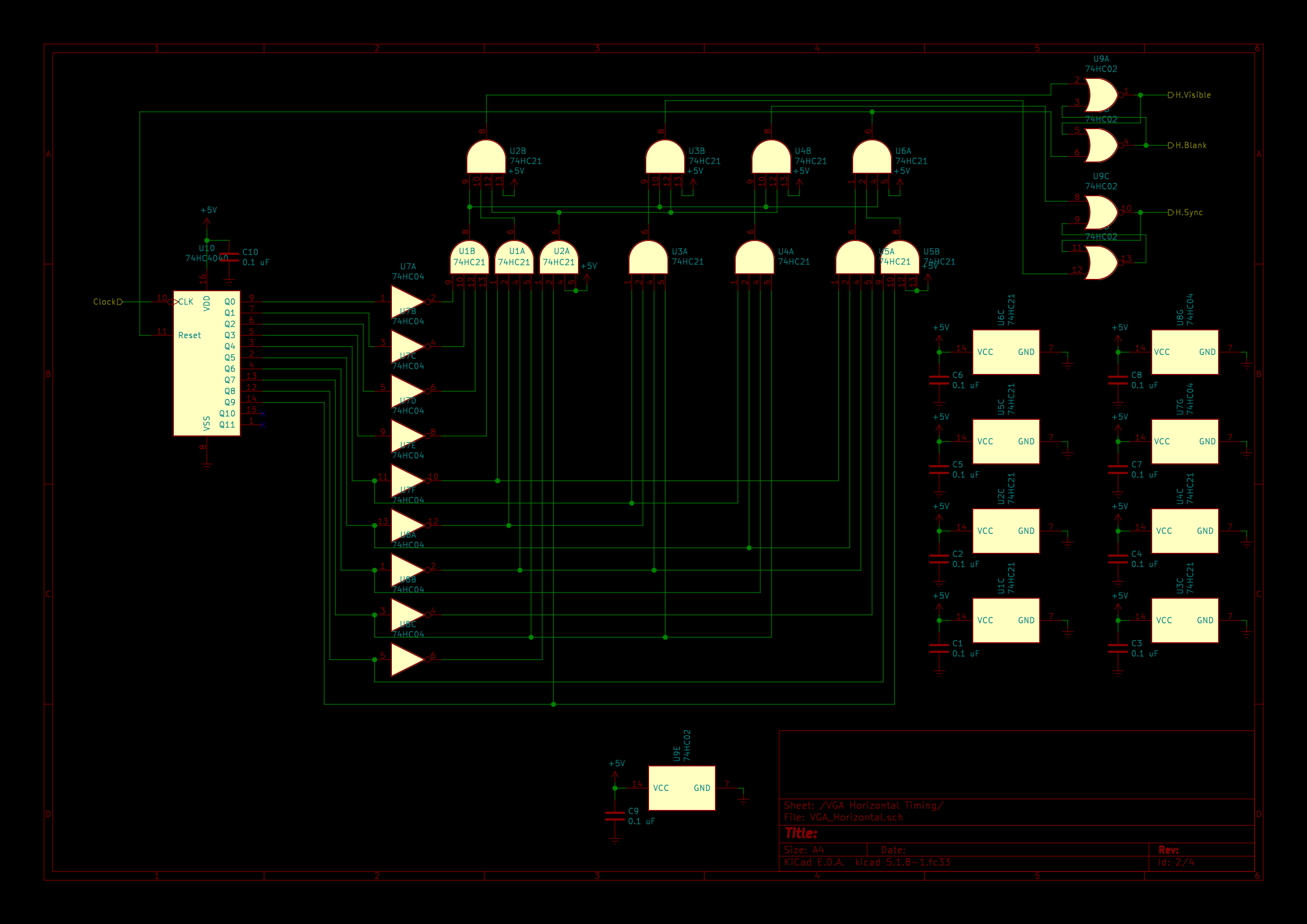
The circuit you see above generates the Horizontal Sync, Blank and Visible signals which partly worked but it turns out I wired it wrong.
Luckily, the soldering and wire wrapping I did right worked as expected. I’ve also got plenty of time and Kynar wire to give it another go!
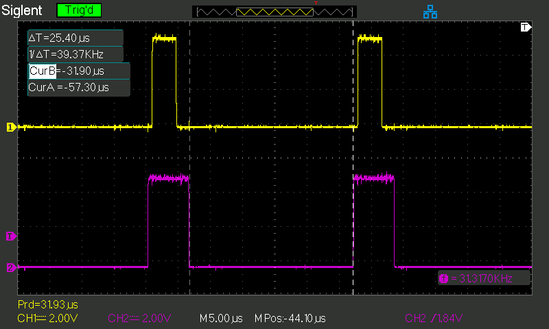
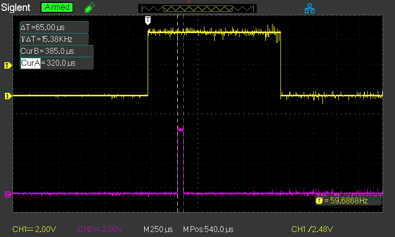
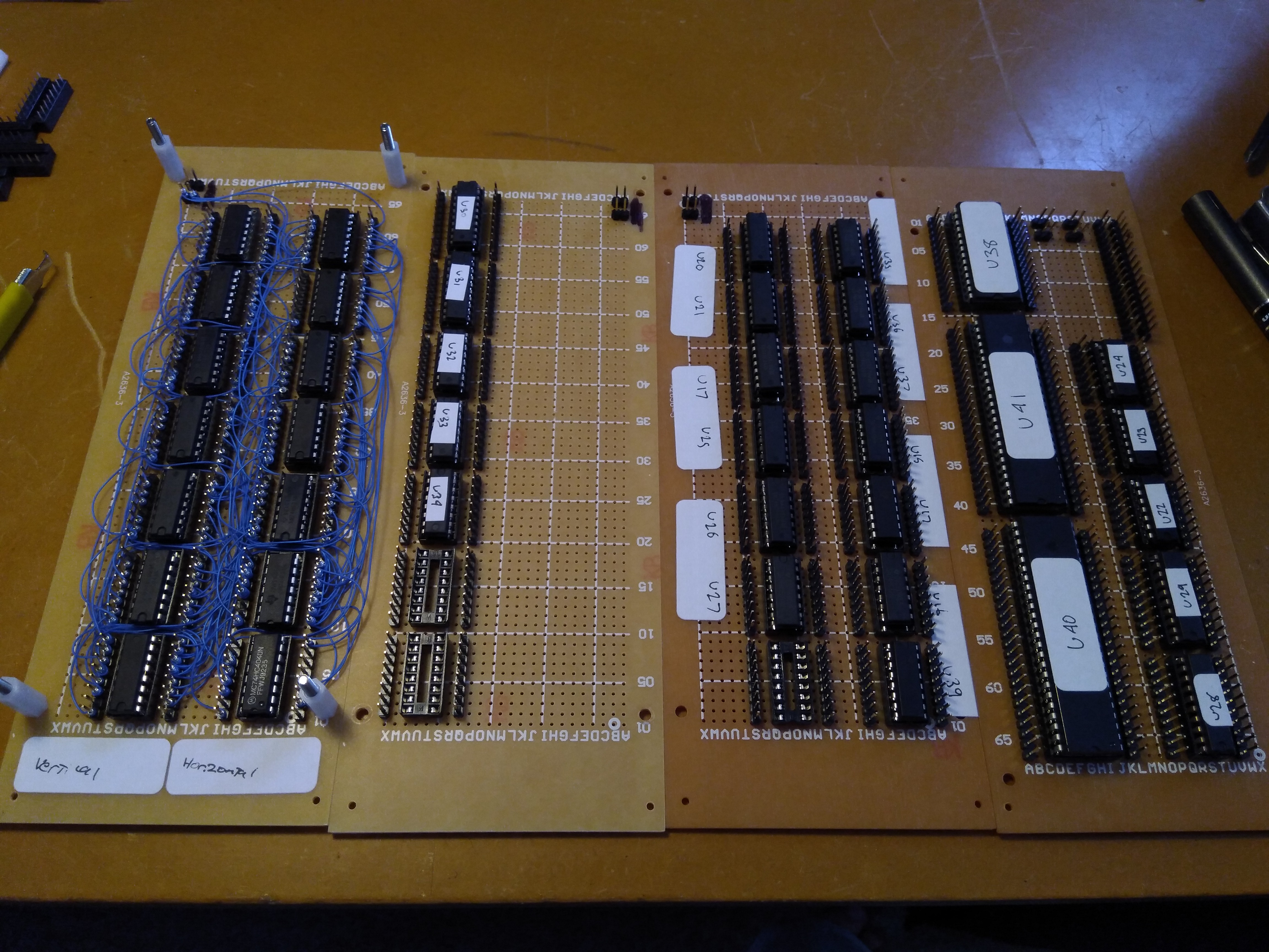
After a lot of confused probing it turns out the circuit works as expected using a slower clock (1MHz instead of 25.175MHz). The reason it doesn’t work with the faster clock is due to the 74HC21 chips not being able to function properly at the faster speed leading to some bad outputs.
What this circuit does is simply count up and activate the Horizontal Sync, Blank and Visible outputs once a certain number is reached according to the VGA specs and so is critical for the rest of the circuit.
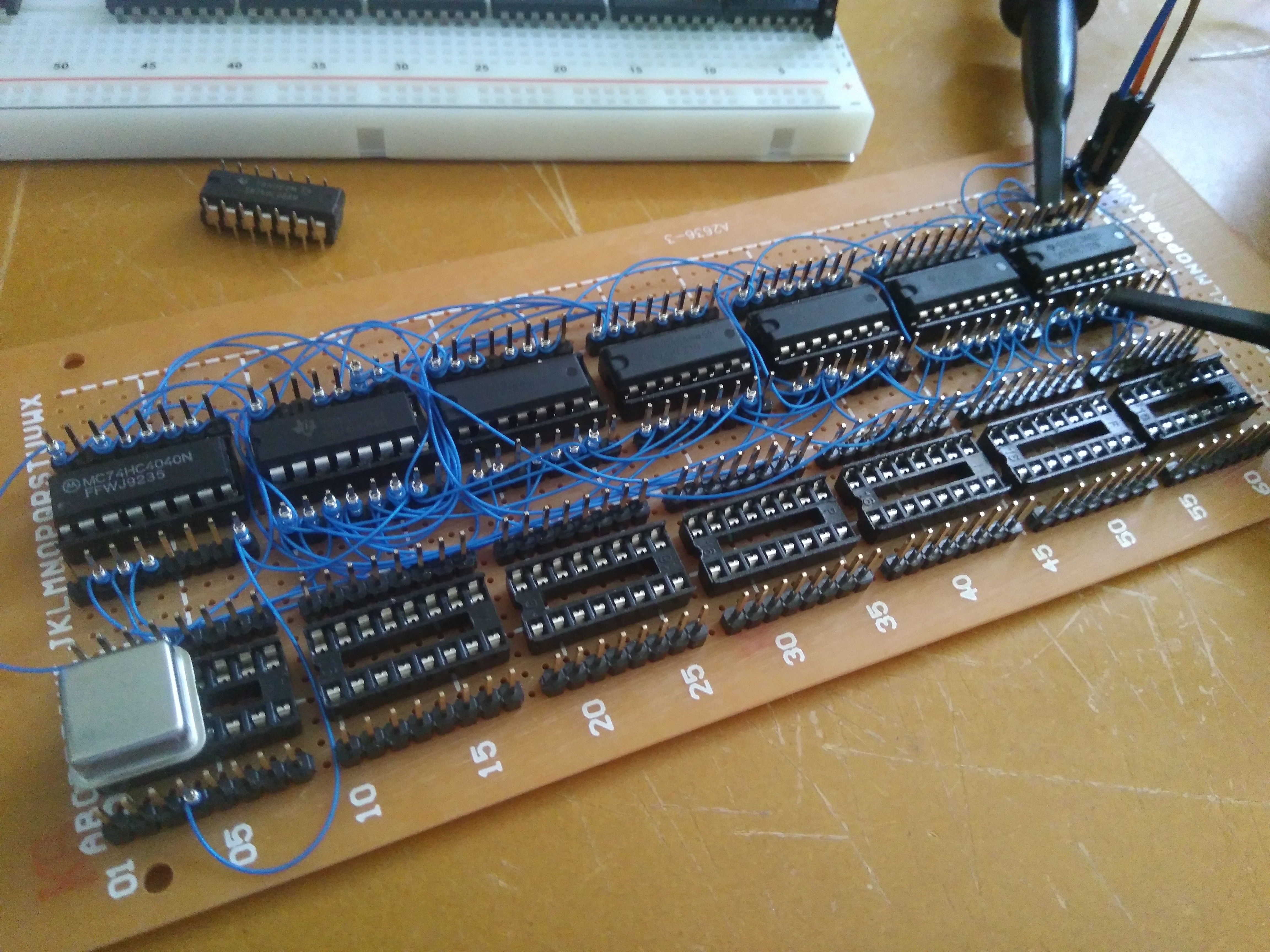
This doesn’t ruin everything though as it turns out I don’t need to check the lower four bits of the count as they are all 0 for each of the numbers I have to check:
This means that the impacted chip can simply be removed without impacting the rest of the circuit! It also means that the chip count can be reduced by a few chips. This is quite possibly the best case scenario.
Revised circuit works a treat! Getting a nice 3.8µs Horizontal Sync pulse and a 25.4µs Horizontal Visible area. All of the other timings are correct too.
Now onto the Vertical Timing circuit!
(If you want to have a look at the circuitry I’m following, Here it is. You can open it in Logisim)
I’ve been watching the Ben Eater videos as well. I know enough to understand the video explanations, but not enough to understand just a circuit diagram (at least for something at this level of complexity). So are you using a similar thing with disabling the CPU while the video is active and letting it run during the blanking, or are you doing something more advanced?
I’m going to do something a bit fancier! I’m planning on using a dual-port SRAM chip so that the graphics card can read from it at the same time as the CPU is writing to it so no clock cycles will be wasted. The ultimate goal is to create a software controllable 40/80 column by 25 row text display so only 2kB of SRAM will be needed for it (80x25=2000).
That’s the next step for this card, now I have to make the character decoder which will work out which row and column of which character to display. Already got a schematic just about worked out just need to do some testing.
So the graphics card actually is a GPU, turning the text into a video signal. Rather than the CPU creating all the bits for the screen and the graphics turning that into a vga signal.
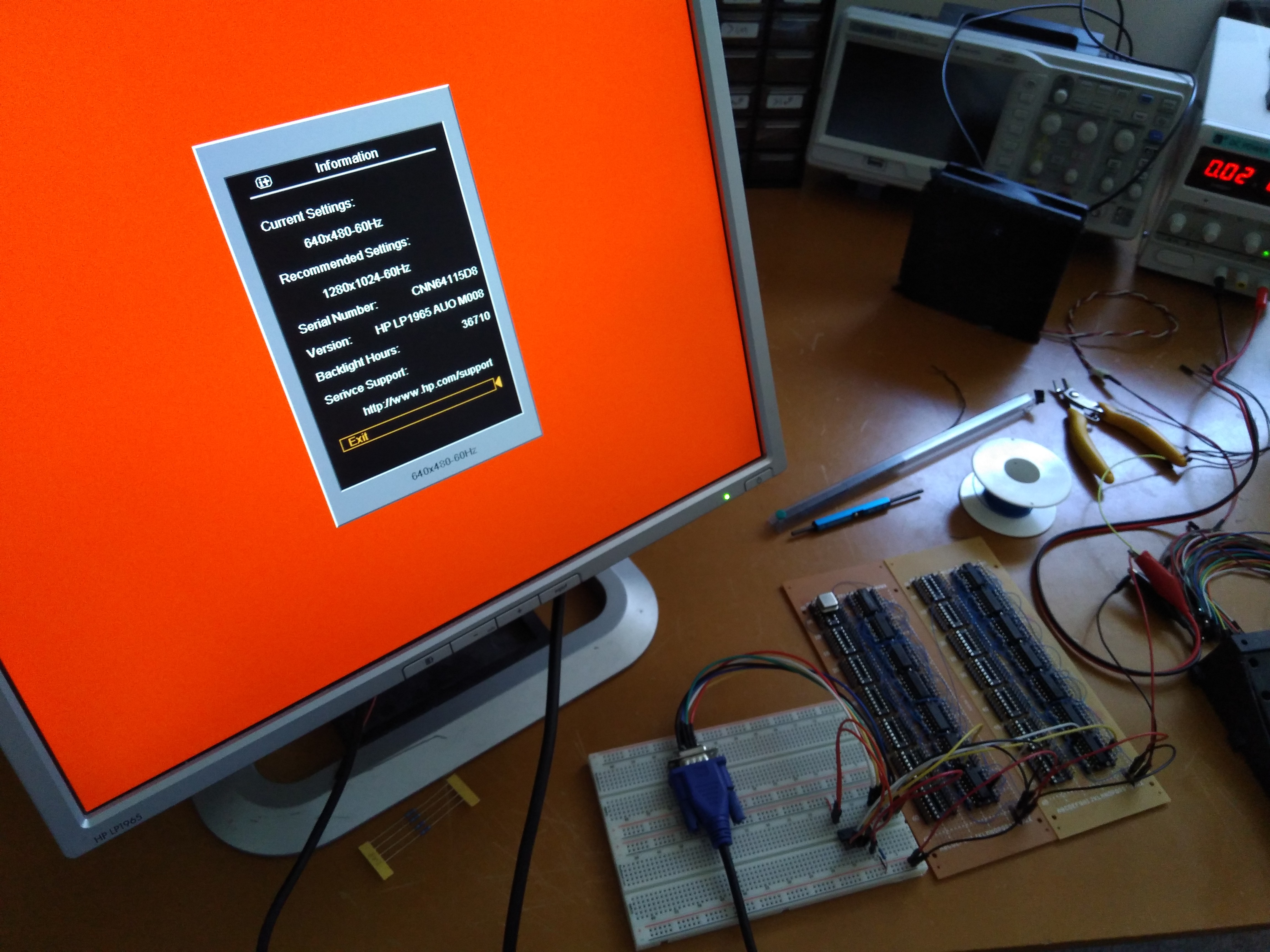
Now that the timing circuits are done, it’s time to work on the character decoder. Right now I’ve out together a circuit to convert 4 bits into a 4 pixel long signal and it’s way cleaner than I was expecting it to be! Practically no fuzziness or flickering that I could see.
The two lines are a single pixel, I’m testing on a 1280x1024 monitor.
Unfortunately I lost one of the chips I need (8 to 1 line multiplexer) so I had to make my own out of some AND, OR, inverter and de-multiplexer chips but it seems to work fine. While I wait for the new chip I’ll work on the schematic for the character decoder.
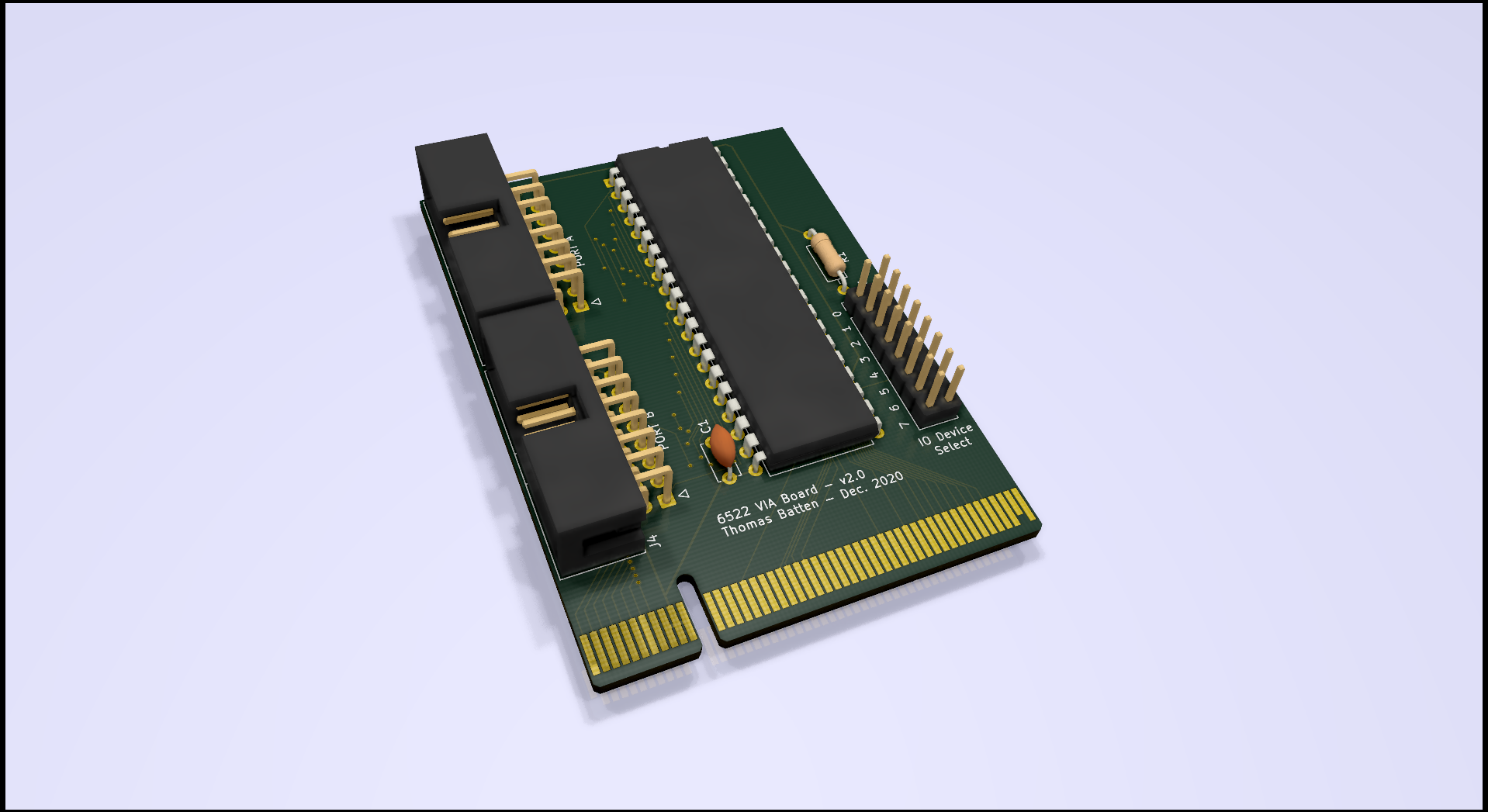
I’ve been doing some work on some updated PCB layouts. The 50 pin connector makes inserting and removing cards far too difficult. I have decided to redo the cards I’ve done using a PCIe 8x card edge connector as make sure that they’re (mostly) smaller than 100x100mm to get them done cheaper at one of those PCB printing places:
DMA yeah, the GPU will have it’s RAM on the card which is connected to the main address and data bus and accessible within a specific address range (See the “memory map” on the system board and the “IO Device select” header on the one below). The GPU will only be able to see the RAM it has on board.


