Dang… Frozen driver stack aside. For a turnkey solution that is hard to beat… Assuming you had 240v just handy to plug into.
For 4xV100 boards, I’m seeing more supply of Fujitsu CX400M4 units but always with 4 16GB V100 units installed. The spec sheet specifies compatibility with 32GB units but pulling the trigger on the board and 4x 32GB units is way out of my budget atm.
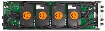
There’s also Dell C4130/4140 boards but there’s like a dozen configurations listed that changes how the backlane presents the GPUs to the mainboard, plus I believe the wiring and coolers are bespoke to that system (but it is quite a bit cheaper and available bare compared to the CX400M4s).
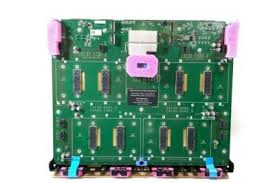
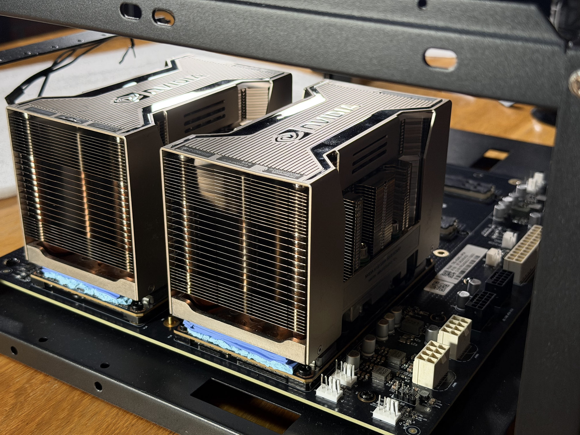
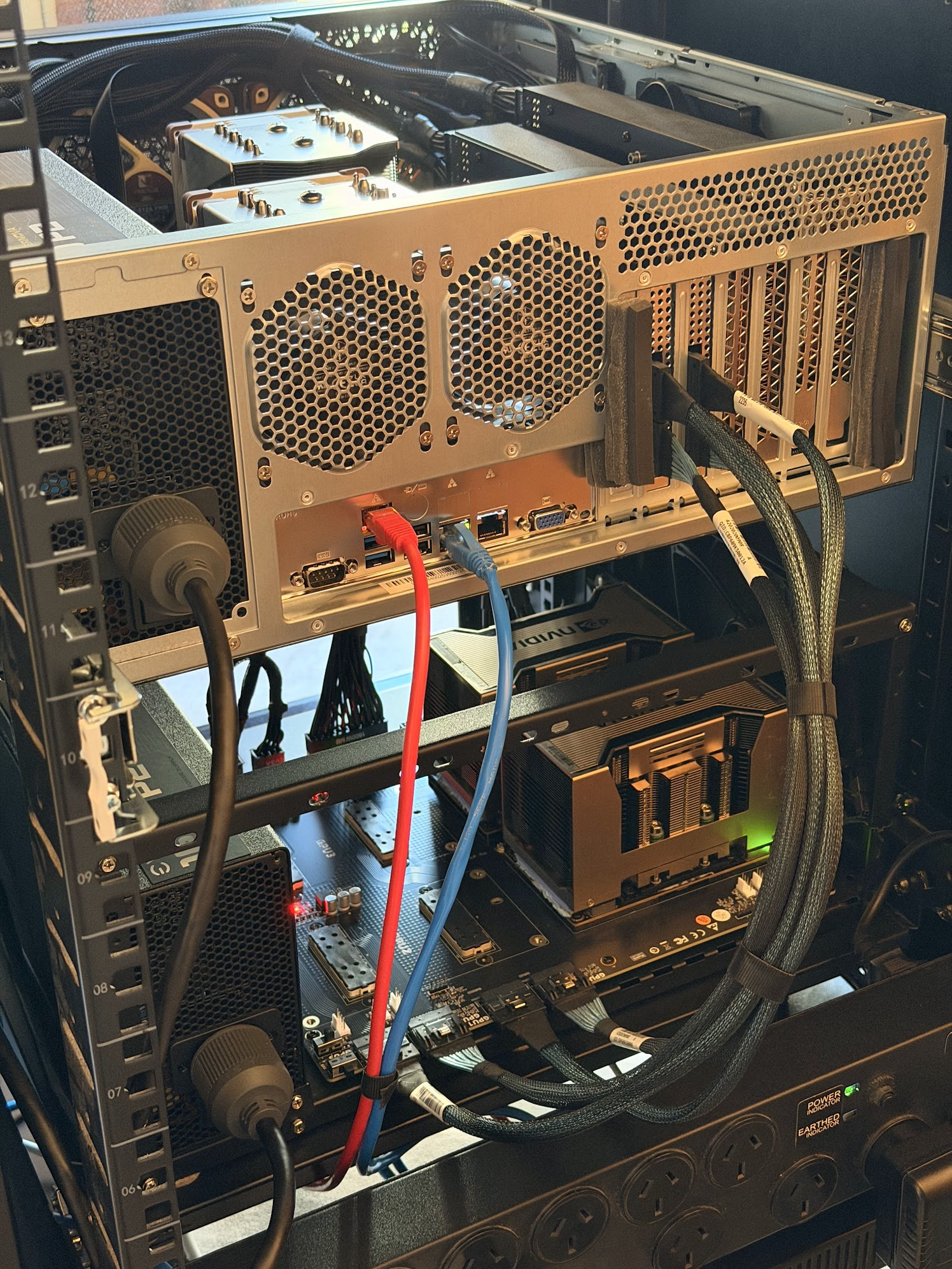
I go this carrier board from Taobao, I believe this is the One Cat AI reversed engineered board, so far 2 V100 it really works in NVLink. I am waiting for a few more GPUs and heatsinks and run as 4 V100 NVLink

3 Likes
That board layout is ideal! Somehow that has slipped past me research.
(the comments show one ontop and a case, total janitor style)
“https://www.taobao.com/list/item/V1Mxdnh3N2VLc0o0dHB1MEZPL3QxUT09.htm”
I don’t know if you are still working on this, but I found some things that might be useful.
oshwhub.com two v100 sxm2 with nvlink on a pcie x16 card
Single V100 on a pcie 16x with a nvlink bridge
I thing a 4 gpu full mesh that each gpu has two SFF-8654 SlimSAS connectors to give full x16 pcie would be quite interesting. Could us 4 PCIE X16 to dual SlimSAS 8i on a hedt, or two of the 6 port PLX88096 switch cards. Or even one of the 10 port PLX88096 cards.
Yep, still working on this!
Testing a 2 x V100 version at the moment, a little like the one you linked from oshwhub.com but with full NVLink between the two GPUs…not sure why that person opted just for 200gb….assume they ran out of layers or space?
And if that works, then it’s an easy port over to 4x v100 with SlimSAS, mapping out the 12 NVLink connections for the 4 cards has been interesting- not often I need spreadsheets for a PCB design! 
Hello. I ran across this thread looking for info on SXM V100s. I would be very interested in an 8x (or more!) V100 SXM2 board. I think V100s and DDR4 platforms are going to be the best hardware mere mortals can expect to get in any quantity for the next few years at least.
Reading through the thread I had a few questions if you’ll indulge me.
This might sound stupid but you said V100’s only have 6 NVlink, uh, links. Could you make a board with 7 gpus and each has 1 link to all the others? Or would that setup make the trace layout too awful? And as a followup what’s the ultimate goal of a layout? Is it least hops for latency?
Can you explain this a bit more? From the reading I’ve been doing it just seems like HCM is 8 cards with NVlinks in a specific configuration. I know the full crossbar thing has more hardware for the fabric but is there something I don’t know about for HCM?
not going to quote the entire post
It’s been mentioned but have you considered PCIe versions past 3.0? If the switch can go up to 4.0 on interface while doing 3.0 on another it seems like it would just work. Get the 4.0 version of a PEX8749 and then 3.0 x8 to each GPU and 4.0 x16 to the host. Then you’re not bottle-necked right? You could also do 3.0 x16 to each GPU and 5.0 x16 to the host but that’s probably too expensive.
Lastly a bit off topic but is there a way the OEM 8x V100 SXM2 boards can be powered independently so you can connect them to arbitrary systems? Like the atx power jumper trick but for server PSUs? Or are they generally locked to the server model they come in?
Not a stupid idea at all, 7 GPUs is actually a really neat special case for V100.
Each V100 has 6 NVLinks and, with 7 GPUs, exactly 6 peers, so in theory you can make a full mesh where every GPU has one direct NVLink to every other GPU.
The trade-off is that you’re spreading those 6 links out.
Each GPU still has 150 GB/s of aggregate NVLink bandwidth each way, but any individual GPU pair only gets one 25 GB/s link (not massively above PCIe 3.0 x16 at roughly 16 GB/s each way).
So, the goal isn’t just “fewest hops”; it’s a balance of hop count, bandwidth between peers, contention, collective performance and how awful the PCB is to route. A 7-way full mesh is logically very elegant, but 21 high-speed NVLink connections would make the board layout pretty nasty.
There’s also a downside when it comes to software (really not my strong suit!). NCCL is topology-aware, so it should in principle discover a non-standard 7-GPU mesh, but I’d want to prove that on real hardware. And 7 GPUs is a slightly awkward number higher up the stack, since a lot of tensor/model-parallel workloads fit 2/4/8-way splits much more naturally.
So: very cool topology, and absolutely worth considering, but I’m not convinced it beats a more conventional 8-GPU layout once bandwidth, routing and software are all taken into account.
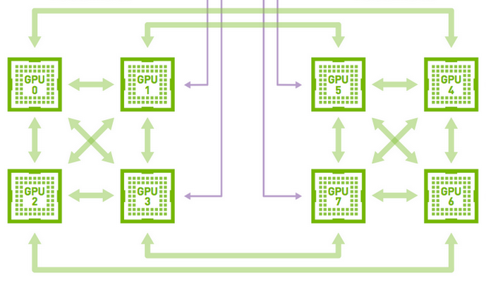
Regarding HCM, you’ve basically got it! My mistake, as I compressed two separate issues there and made it sound like HCM itself needed extra fabric hardware, which it really doesn’t, as the hybrid cube mesh is fundamentally just 8 V100s with the 24 NVLinks routed in NVIDIA’s specific topology. No NVSwitch or hidden crossbar is required.
What I meant by “closer to a DGX-style baseboard” was the PCB complexity around doing that properly. You’re routing hundreds of very high-speed differential pairs between eight SXM2 modules, so suddenly controlled differential impedance, intra-pair skew, pair-to-pair length matching, reference-plane continuity, return paths, crosstalk, via transitions/stubs and ground stitching bla bla bla all start to matter.
Then you still have the PCIe fabric, clocks, management and a pretty serious power-delivery problem to fit around it.
That’s the point where the board stops looking like a fairly straightforward open 4-GPU backplane project and starts looking like a proper high-speed server baseboard with a much nastier stack-up and routing problem, talking orders of magnitude more work for a project.
So I’d correct my original wording to: “8× V100 HCM is absolutely possible without extra fabric, it’s just substantially harder and more expensive to lay out and manufacture well than the 4-GPU design.”
Also keep in mind I am not an expert in ANY of this; I am just poor and competent with PCB design!!!
Have you though of SXM3 There are only the single card adapters currently and no proper backplane. That seems to be keeping down the price of the SXM3 V100s. https://www.ebay.com/itm/278138489934
I have though about a 8x v100 system made out of two 4x backplanes connected by two PEX88096 that have a x16 link to allow gpu to geu traffic between the backplanes.
                     HOST / ROOT COMPLEX
                        |           |
                        |           |
                 Gen4 x16       Gen4 x16
                        |           |
                        v           v
                   +--------+   +--------+
                   |  PEX1  |<->|  PEX2  |
                   +--------+   +--------+
                       |             |
                       |             |
                     64 lanes      64 lanes
                       |             |
                       v             v
                  BACKPLANE 1   BACKPLANE 2
                       |             |
                    G0-G3          G4-G7
                    NVLink         NVLink
                     mesh           mesh
My thought/ hope was to use the PEX88096 cards, but I haven’t found any information on connecting two together. The literature for the PEX88096 describes it but not in the detail/ understanding that I am willing to risk. I will keep on digging. I understand that it is host/root complex bandwidth limited, but that is just a though on how to get a 8 gpu system with two gpu backplanes. Allowing the same backplane to be in different configurations.
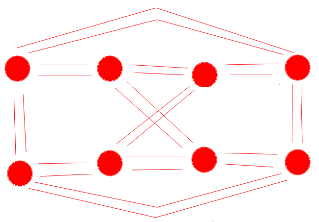
Out of interest do you know what the actual HCM topology is? I’m guessing the topology for 4 gpus is one of these but I can’t think of a way to make 8 in a 2x4 grid distribute nicely and use all the links.

Edit - I decided to stop being lazy and answer my own question.

It seems like they’re only using 4 of the six links per card? I can get it so everything has a 2x link so double the bandwidth and for each gpu there are 3 neighbors, 3 gpus that are one hop, but a single gpu that’s 2 hops.
In any event if you do decide to make a 8 gpu board with ATX power and a good (50GB/s+ total) PCIe uplink within the next year or so I would easily pay $1000 for one. And keep in mind the V100 can be power limited to 150w with minimal performance loss which means you could run a full board of 8 of them off one 120v/15A circuit and PSU.
My current setup can not run all the GPUs at full power either but I have it set to run nvidia-smi to limit the power on boot and it works fine.

I wonder if what you found is a simplification of this. That image is from. NVIDIA Tesla V100 Volta Update at Hot Chips 2017 This is a later look at it with hardware. Gigabyte G481-S80 8x NVIDIA Tesla GPU Server Review the DGX1.5
So nvidia switched up their topology too huh?
@peps1 Something I was wondering, how much of a savings is it if none of the NVlink connections cross each other? Does that let you save on PCB layers?
Edit - actually looking at my previous suggestion I think all GPUs can be reach from anywhere with one hop?
Apologies for the double post but I was thinking about this a bit more.
You probably already had this in mind but I just hadn’t made the connection - if you have passive PCIe links via SlimSAS from each individual gpu you could just drop the SlimSAS connector right next its GPU. Meaning you don’t need to have the PCIe traces cross an NVlink traces in the PCB so you can cut down on PBC layers, right? If that’s the case I think you’re right about passive being the way to go.
I was also thinking if you had two SlimSAS 8i connectors per gpu then you could get the full x16 from each but also people with less PCIe lanes could just use one connector for x8. I don’t know how much an extra connector is but it would make the board very flexible.
Additionally I don’t think there’s much difference between passive x4 and x8. Workstation and server boards that support bifurcation are going to do x8/x8 or x4/x4/x4/x4 and would have the lanes to do x8 for each GPU. Consumer boards with limited CPU lanes will be lucky to get 4 physical PCIe slots and none of them will run at more than x8 with four slots populated so people on consumer boards are just going to plug in one SlimSAS connector to each slot and use whatever lanes the slot has available.
Finally I had one crazy idea: I don’t know enough about signaling requirements to check but two SlimSAS 8i cables have 16 wire pairs, and one NVLink is also 16 wire pairs. What if you were able to have multiple 4x V100 boards connect to each using SlimSAS cables? It would be a lot of cables, sure, but I wouldn’t have any qualms about it.
Yes / maybe.
It was something I considered early on, as the makers of SlimSAS actually claim NVLink support. I was looking at using it for a single SXM2-to-PCIe carrier PCB holding one V100, with the NVLink interfaces broken out to SlimSAS so multiple identical boards could be linked together.
The problem was the number of cables. If one SlimSAS 8i carries one complete NVLink, fully using all six NVLinks on each GPU means 6 cables for 2× V100s, 9 for 3×, and 12 for 4×.
I never got those PCBs fabricated because, once you add up the connectors and cables, it starts becoming cheaper and cleaner to just make a larger PCB with the NVLink routing built into it.
But….That said, the electrical side did look surprisingly promising. Amphenol explicitly lists SlimSAS as supporting NVIDIA NVLink at 25G, so this isn’t just assuming a storage cable happens to have enough differential pairs. It seems the interconnect was actually designed/rated with NVLink-class signalling in mind. That doesn’t guarantee a DIY V100 implementation will work without signal-integrity testing, but it makes the idea a lot less crazy.
My designs for the 4-card version just use 4 SlimSAS connectors one PCIe x8 connection per V100.
I don’t think there’s much benefit in trying to give every V100 a full PCIe x16 connection for this sort of system. PCIe is important for getting the workload/data into the GPUs in the first place, but once the model/data is resident in VRAM, the GPUs should be doing their GPU-to-GPU communication over NVLink, not bouncing it back through PCIe and the CPU.
A V100 has six NVLink 2.0 links giving up to 150 GB/s in each direction of aggregate GPU-to-GPU bandwidth, whereas PCIe 3.0 x8 is only about 8 GB/s each direction. So once you’re actually running a multi-GPU workload, the NVLink fabric is vastly more important than whether each individual GPU has x8 or x16 back to the host.
There are obviously workloads that constantly stream data between system RAM and the GPUs where x16 would help, so PCIe isn’t irrelevant, but for the sort of multi-V100 compute/LLM setup this board is aimed at, I think spending twice the PCIe lanes just to give every GPU x16 has pretty poor returns.
Wow! really?! That’s crazy that they officially support a proprietary standard like that. I mean, is NVLink-over-SlimSAS even used anywhere in an OEM product lol?
I was kinda mixing ideas in my earlier post. I thought the bandwidth would useful if it was just two independent V100 x4 boards both connected to the same PCIe root. That 64GB/s might be enough to still do worthwhile parallelism between boards (and to a lesser extent hybrid GPU/CPU work). Ice Lake is DDR4 and has 64 PCIe lanes per socket… Then again you’d need double that for both boards, meaning 128 lanes, so I think I’m just completely wrong?
After checking it looks like some of current intel server cpus have more than 128 lanes… but no one is going to be dropping 5 figures on a granite rapids CPU to connect some V100s over PCIe 3.0 a bit faster. I don’t know what I was thinking.
Agreed.
I think it’s only half as many pairs and that’s why it’s rated at 25G - I said it earlier but I used “two” instead of “2” for whatever reason.
Ultimately even more than an 8x V100 board I’d love to see 4x boards that could be connected together semi-indefinitely with SlimSAS connectors. I haven’t really thought it out so I’m sure there’s a better topology but naively if we assume these are all 1x NVLinks:
Then for 8x V100 it would only be 8 SlimSAS cables total or 1:1 with the cards (instead of 3:1 lol) and mirror an official topology. The additional cost would be just 2 extra SlimSAS connectors per card.
You could even try and Frankenstein 3 or 4 boards together with reasonable-ish topologies!
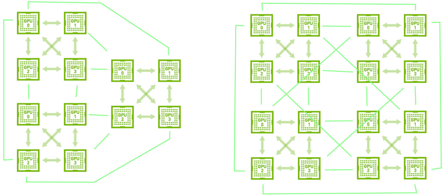
I don’t even know if this would work but could you imagine it! Half a TERABYTE of unified-ish VRAM for under $10,000! HALF the cost of a SINGLE RTX6000 PRO! I don’t care if it would be a rats nest of wires on a table, take 2400w minimum, and might not work, I would absolutely try this.
Hello everyone.
Seen this topic I had an idea. why not try a modular approach ? divide the PCB like this :
1 PCIE x4 card for each v100 that connects only first sxm2 connector (maybe through SFF connector)
A nvlink connector that aggregates 2x or 4x card or 4x+2SFF connector for expansions
the good point is that everyone gets what it wants the bad point is that mechanically is probably a mess.
Anyone interested in this ?
I mean, I love a bit of modularity. My only real concern is trying to do NVLink through a separate bridge PCB.
The proper NVLink carrier/bridge hardware is crazy expensive, and I still haven’t found a DIY bridge design that’s been conclusively demonstrated working. The closest I’ve found is a DIY “100G” bridge for V100 SXM2 adapters, but even there it’s unclear whether the NVLink connection itself was ever successfully brought up — the author definitely got the GPUs working over PCIe, but I haven’t seen an nvidia-smi nvlink result or bandwidth test proving the bridge worked.
And doing it between two cards is already a fairly nasty high-speed PCB problem. You’re dealing with controlled differential impedance, tight pair matching, via/connector discontinuities, reference planes and keeping the signal paths short and consistent. Once you start trying to interconnect three or four cards, the routing problem gets much worse because you’re multiplying the number of high-speed paths that all have to meet those constraints.
That’s why I’m much more confident in a modular approach for PCIe/power than I am in making NVLink modular. NVLink is the bit where I’d really like to see somebody prove a DIY bridge works reliably before committing a lot of money to PCBs.
But I will fire up the Chinese VPN, and see if there have been any new developments.
The main point for me is exactly this: the nvlink and all the rest (pcie power suplly etc..) have different requirements. The problem is the dissipation factor of FR4 at 10ghz (nvlink should work around this frequency). I would like to go with JLCPCB due to low cost. With the S1000-2M material and backdrill, from my computation we could have 12/15 cm of reliable connections, that could be enough. Also to reduce cost in my opinion it is good to have one standard board for pcie, and one dedicated for nvlink that in case of unreliable connection can be swapped with one with better materials.
1 Like
Hello again,
does anyone have the full pinout of the Nvlink connector ?
Do you actually have a good source for info on the 1CATai developments? The best I’m aware of is this The Most Esoteric eGPU: Dual NVIDIA Tesla V100 (64G) for AI & LLM
I gotchu Reverse Engineering the NVIDIA SXM2 Socket | Benchoff Design Portfolio . I actually already had this open.