Designing an open-source budget 4x V100 SXM2 NVLink backplane — passive PCIe vs PEX8749?

Hi all,

I’m working on a possible open-source/barebones backplane for 4x NVIDIA V100 SXM2 modules.

The rough idea is to make something that people could potentially build or have fabricated themselves, rather than relying on rare and expensive OEM trays. I’m trying to keep the design as cheap and simple as possible, but I want to sanity-check the PCIe topology before I go too far down the wrong road.

The basic assumption is that each 4-GPU PCB/backplane would act as its own NVLink island. So inside one 4x V100 SXM2 board, the GPUs can talk over NVLink, assuming the backplane routing/topology is valid.

The thing I’m trying to understand properly is what happens when you have two of these 4-GPU boards.

So:

4-GPU backplane A = NVLink island A

4-GPU backplane B = NVLink island B

As far as I can tell, there is no simple/cheap way to make those two islands talk to each other over NVLink unless you are basically building a proper NVIDIA/OEM-style NVSwitch/NVLink baseboard. So for a DIY budget design, I’m assuming island-to-island traffic has to go over PCIe.

That means the real design question is not “how fast is each individual GPU to the host?” The model weights live in VRAM, and the GPUs inside each 4-GPU board already have local NVLink. The important question is:

How fast can backplane A talk to backplane B?

This is where I’m trying to decide between passive PCIe wiring and a PEX8749 switched design.

Option 1: Passive x4 / OCuLink per GPU

One 4-GPU board would use one host x16 slot split into x4/x4/x4/x4.

So per 4-GPU board:

1x host x16 slot

4x OCuLink x4 cables

4x GPUs, each with its own PCIe 3.0 x4 link

For two boards / 8 GPUs total:

2x host x16 slots

8x OCuLink x4 cables

The island-to-island ceiling should be around:

4x PCIe 3.0 x4 = about 16 GB/s one-way, best case

This seems cheap and simple from a PCB point of view. No PEX chip, no switch cooling, no switch configuration. But it needs x4/x4/x4/x4 bifurcation and uses a lot of cables.

Also, if the software traffic only crosses between the two islands through one “boundary” GPU, then the real path could be only x4, so about 4 GB/s one-way. If traffic is spread across all four GPUs, then the aggregate can be around 16 GB/s.

Option 2: PEX8749 switched 4-GPU backplane

This is the common 4-GPU PLX/PEX style layout I keep seeing.

PEX8749 is 48 lanes, so the obvious layout is:

1x PCIe 3.0 x16 upstream to the host

4x PCIe 3.0 x8 downstream to GPUs

That uses all 48 lanes.

So per 4-GPU board:

1x host x16 slot

1x x16 uplink cable

PEX8749 on the backplane

4x GPUs downstream at x8

For two boards / 8 GPUs total:

2x host x16 slots

2x x16 uplinks

2x PEX8749 backplanes

The path between islands would be:

Backplane A GPUs
to PEX8749 A
to shared x16 uplink
to host/root complex
to shared x16 uplink
to PEX8749 B
to Backplane B GPUs

So as far as I understand it, the island-to-island ceiling is still around:

PCIe 3.0 x16 = about 16 GB/s one-way

That means two PEX8749 boards are not really faster than passive x4/OCuLink in best-case aggregate island-to-island bandwidth.

The advantage is more practical:

far fewer cables

one host connection per 4-GPU board

doesn’t need motherboard bifurcation

cleaner product/backplane design

probably easier for other people to use

The downside is:

PEX chip cost

heat

PCB complexity

still only one shared x16 exit from each 4-GPU island

Option 3: Passive x8 per GPU

This seems like the only realistic cheap-ish way to beat the 16 GB/s island-to-island limit.

One 4-GPU board would use two host x16 slots, each split x8/x8.

So per 4-GPU board:

2x host x16 slots

4x PCIe x8 links

For two boards / 8 GPUs total:

4x host x16 slots

8x x8 cables

The best-case island-to-island bandwidth would be:

4x PCIe 3.0 x8 = about 32 GB/s one-way

This seems like the best performance/value option on lane-rich platforms like EPYC or Threadripper, but it is obviously messier as a product. It uses more host slots and more cables, and requires working x8/x8 bifurcation.

Again, this only helps if the workload can actually use multiple GPU paths between islands. If the traffic only crosses through one GPU, then you only get one x8 path.

Option 4: Passive x16 per GPU

This is mostly just a reference point.

For two 4-GPU boards, you would need:

8x x16 host lane sources

8x x16 cables

That would give a theoretical island-to-island aggregate of:

4x PCIe 3.0 x16 = about 64 GB/s one-way

But this is not realistic for most people and not really relevant to the budget/open-source goal.

Where I think I am currently landing

For a cheap open-source design, my instinct is:

Base design:

passive board

ideally x8-capable

allow x4/OCuLink as the cheaper/dense mode

Optional premium/easy wiring design:

PEX8749 switched version

one x16 host uplink per 4-GPU board

cleaner and easier for users, but not faster island-to-island

So my current mental model is:

passive x4/OCuLink:
cheap, simple, about 16 GB/s island-to-island best case

2x PEX8749 boards:
cleaner wiring, fewer host cables, also about 16 GB/s island-to-island

passive x8:
more cables and host slots, but about 32 GB/s island-to-island best case

PEX8796 or larger switch fabric:
interesting, but probably too expensive/complex for the kind of project I’m aiming at

NVSwitch / true 8-GPU NVLink fabric:
probably not realistic unless reusing or cloning an OEM-style design

Questions

Am I right that two separate 4x V100 SXM2 NVLink backplanes cannot practically be bridged together with a simple DIY NVLink PCB?

Am I right that, for a budget design, island-to-island traffic should be assumed to go over PCIe?

With two normal PEX8749 4-GPU boards, is island-to-island traffic basically limited by the shared PCIe 3.0 x16 uplink from each board, so around 16 GB/s one-way?

Is passive x8 per GPU the only realistic budget way to get meaningfully more island-to-island bandwidth?

Are there any PCIe switch options I’m missing that are faster than PEX8749 but still not silly money?

For LLM inference across two 4-GPU NVLink islands, does the theoretical passive x8 aggregate actually matter in practice, or do frameworks often end up bottlenecking through one or two boundary GPUs anyway?

If you were designing a barebones DIY/open-source 4x V100 SXM2 backplane, would you prioritise:

passive x4/OCuLink for lowest cost,

passive x8 for better island-to-island bandwidth,

or PEX8749 for cleaner wiring and broader host compatibility?

My reflex is always to make the cheapest useful option for the end user, so I’m leaning passive unless there is a strong practical reason to use PEX. I just want to check I’m not missing something obvious before I design the board around the wrong assumptions.

1 Like

Is this the kind of thing you are talking about?

These things are real affordable and do work, popping up on ebay. In my opinion they are past due because the software support is leaving older pre-ampere generations behind. This is going to be your biggest hurdle rather than making the hardware work.

1 Like

Yes, that kind of thing, but considerably cheaper, and Open.

In my opinion they are past due because the software support is leaving older pre-ampere generations behind.

Still a excellent option for entry level IMHO with things like the forked FlashAttention support they are remaining useful for the homelab and learning, as reflected in the bounce back on pricing in the used market.

I have zero knowledge of NVLink, so here is a n00b question: What the “physical” interface of NVLink looks like?

For all practical purposes, if you have a PCIe Switch big enough then you could connect all cards PCIe to it and for PCIe P2P purposes they could all “see” themselves, then the PCIe Switch uplinks to the host. But NVLink is supposed to be a separate direct sidechannel connector between cards, albeit I think they introduced a switch/router topology for bigger multiGPU deployments. So, is NVLink a protocol on top of PCI Express, or is something completely separate? Can you connect this NVLink sidechannel to a standard PCIe Switch, or you need specialized silicon for the NVLink switch/router chip that you need to procure somehow compared to off-the-self PLX PCIe Switches?

I mean it is a good question!

NVLink on V100 SXM2 is basically a set of very high-speed point-to-point links between GPUs. It’s not really like PCIe where you can just add a generic switch/card/cable and expect everything to be happy.

Physically, from a PCB point of view, Its high-speed differential routing: controlled impedance, tight length matching, clean reference planes, careful via use, clock managed and preferably a very unforgiving layer stackup. So yes, electrically it is “just copper traces” in one sense, but not in the casual sense.

The topology is the bit that matters, though with the V100.

Each V100 SXM2 has 6 NVLink links. Each link is point-to-point and is about 50 GB/s bidirectional, so a V100 has up to 300 GB/s bidirectional aggregate NVLink bandwidth.

That makes a 4-GPU board much more realistic than say an 8-GPU full mesh. With 4 GPUs, each GPU only needs direct links to 3 other GPUs if you want a fully connected island, so the link count is manageable.

With 8 GPUs, a true full mesh would require each GPU to connect directly to 7 other GPUs, but V100 only has 6 NVLink links. So you run out of links before you can do a simple all-to-all 8-GPU PCB.

You can stop reading here if you want :slight_smile:

But………That doesn’t mean 8-GPU V100 systems are impossible. DGX-style systems did 8x V100, but they used a specific hybrid cube mesh topology rather than a simple full mesh. That is a much bigger design problem, because now you are trying to reproduce a known topology that the NVIDIA software stack expects, not just connect every GPU to every other GPU.

So, for a DIY/budget backplane, my current thinking is:

4x V100 SXM2 NVLink island = maybe realistic as a research/DIY PCB, cheap, works, lovly 300 GB/s bidirectional on all cards

8x V100 SXM2 full NVLink mesh = Not possible.

8x V100 SXM2 using a hybrid cube mesh = possible in principle, but much closer to cloning a DGX-style baseboard than making a simple open-source backplane, resulting in a much more expensive build that is not going to benefit a fraction of a per cent of people over a 4 card NVlink setup that can be expanded to a 8 GPU if really needed at the cost of loosing NVLink between the two isalnd of GPUs.

For all practical purposes, if you have a PCIe Switch big enough then you could connect all cards PCIe to it and for PCIe P2P purposes they could all “see” themselves, then the PCIe Switch uplinks to the host. But NVLink is supposed to be a separate direct sidechannel connector between cards, albeit I think they introduced a switch/router topology for bigger multiGPU deployments. So, is NVLink a protocol on top of PCI Express, or is something completely separate? Can you connect this NVLink sidechannel to a standard PCIe Switch, or you need specialized silicon for the NVLink switch/router chip that you need to procure somehow compared to off-the-self PLX PCIe Switches?

NVLink is separate from PCIe. It is not PCIe-over-another-connector, and a normal PLX/Broadcom PCIe switch cannot route NVLink traffic. A PCIe switch can put all the GPUs into one PCIe fabric and may allow PCIe peer-to-peer, but it is still limited to PCIe bandwidth/latency.

For V100, that gap is large. PCIe 3.0 x16 is about 16 GB/s one-way. A V100 SXM2 has six NVLink links, each around 50 GB/s bidirectional, so NVLink is in a totally different class when the topology supports it.

So for two separate 4-GPU SXM2 boards:

Inside each board:
GPUs can use local NVLink, assuming the routing/topology is valid.

Between the two boards:
traffic falls back to PCIe unless you have a real NVIDIA-style NVLink/NVSwitch fabric joining them.

A PEX8749 setup would look like:

Backplane A → PEX8749 A → PCIe x16 → host/root complex → PCIe x16 → PEX8749 B → Backplane B

That means island-to-island is roughly PCIe 3.0 x16 class, around 16 GB/s one-way. Useful, but nowhere near NVLink.

So my current assumption is: PLX/PEX is good for clean PCIe wiring and compatibility, but it is not an NVLink substitute. To route NVLink between islands, you need NVIDIA-specific NVLink/NVSwitch silicon/topology, not an off-the-shelf PCIe switch.

Your explanation about how things are connected in 4 GPU vs 8 inmediately remind me of Xeon Scalable series which had the same compromise about 4 GPUs being fully interconnected, but 8 don’t: Intel Xeon Scalable 2 4 And 8 Socket Topology - ServeTheHome
I believe AMD Opterons also used similar topologies for 8 Socket back when it was a thing two decades ago. Then they scaled down all the way to only 2 with EPYC.

Does such NVLink switch exist, so instead of connecting GPUs directly between them you use a switch and connect all NVLinks to it? I was thiking of something that looks exactly like the PCIe Switch, but based on a different specialized NVLink chip and without host connection. I assume that you can’t get a NVLink switch off-the-shelf…

Yeah, that’s exactly the right. Once you move past a small fully-connected group, it becomes a topology problem, just like old multi-socket CPU systems.

And yes, the NVLink version of what you’re describing does exist: NVSwitch. It is basically NVIDIA’s dedicated switching fabric for NVLink traffic…..but…..

The catch is that it is not like buying a PLX PCIe switch and dropping it onto a board. A PLX/Broadcom switch routes PCIe. NVSwitch routes NVLink. Different protocol, different silicon, and very much tied into NVIDIA’s platform ecosystem, as in you buy everything moy just the Switching.

So in theory, yes: instead of direct GPU-to-GPU NVLink links, you can build a bigger topology around NVSwitch.

Cost-wise, that is the killer. Used PLX/PEX PCIe hardware is relatively accessible. NVSwitch hardware generally comes as part of expensive OEM baseboards/systems, not as a cheap off-the-shelf hobbyist part. Even if you could salvage the chips, the PCB and validation work would be a major project.

So….

yes, the thing exists, NVSwitch!

yes, conceptually, it is the NVLink equivalent of a switch fabric! (and I still think even talking conceptually its still cool!)

no, it is not realistically comparable to using an off-the-shelf PCIe switch :face_holding_back_tears:

1 Like

Nvidia developed NVLink because there was no chance to achieve NVLink speeds with PCIe.

1x Broadcom PEX88096 per 4 GPUs (4x PCIe 3.0 x16 (64 lanes) → 2x PCIe 4.0 x8/x8-bifurcation (32 lanes)) is probably the only way to get full bandwidth of all GPUs in parallel. 8 V100 would need 4 x8/x8 bifurcated PCIe 4.0-slots on the host mainboard.

I’m here to learn about the methods your describing. You want to make a NVlink 4 GPU system for consumers? That plugs into PCIe? is it 1 GPU to 1 PCIe 4x?

Outside of the ridiculous price difference(between SXM2 and PCIe cards that is), what’s the upside of making one over using the ones on the market?

Just interested

Yes, I agree with that. But given the models live in VRAM using NVLink between 4 GPUs at a time, trying to give each GPU x8 via a PEX88096 just to maximise per GPU bandwidth over PCie seems like a very diminishing returns when it comes to price/performance.

The key connection would be between the two islands of GPUs, where you have to come back to the host PCIe rather than using NVLink.

Well, not consumers, but for people to make themselves as a cheap, accessible option, think homelab, students doing Data science or Computer science, the current options are quite expensive for what they actually are (due to demand, and Chinese manufacturing struggling to fulfil the needs of the domestic market, let alone an international one)

Yes, it’s what is known as a “backplane” A PCB that holds 4x V100 SXM2 GPUs that are all linked via NVLink (this makes communication between the cards much faster than having 4 cards on 4 different PCIe slots) and only uses 1 PCIe slot on the host.

It’s purely a question of cost, along with the ability to change and modify to fit each person’s needs. The market is very strange right now due to global demand and a handful of factories that can’t keep up with domestic demand, which pushes prices up in international markets.

These backplanes, from a bill of materials standpoint, are nothing complex: power filtering, buck converter circuits, clocks, fuses, microcontrollers for fan controls and connectors, the price reflects supply and demand, not the BOM cost.

I personally feel that being able to get something like this into the hands of students at a fraction of the price would be a good thing.

1 Like

Re card to card traffic moving between pcie bridge domains:

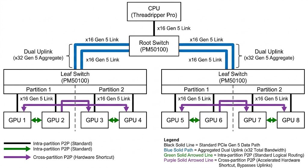
This is a mostly solved problem between NCCL topology selecting the optimal traffic pattern and breaking physical switches into multiple different partitions giving you double-x16 to the upstream (either root switch or CPU) means you are effectively getting a nonblocking pcie gen5 communication flow in this exact setup for TP8 VLLM or SGLANG usage.

2 Likes


Asked an eBay seller about how these boards function. Seems you do get NVlink between GPUs but only 8X per GPU to the switch/CPU.

Not great, not terrible.

Now if @peps1 wanted to make A LOT of friends, they could look into making a board for the MI250X.

That would be sick.

2 Likes

Apparently the older AMD stuff would be simpler than trying to re-implement nvswitch (or worse, Gaudi style dozens-of-100gig-ethernet links between GPUs)

Should just be copper traces and possibly some kind of redriver if signal drops too low.

2 Likes

Wow it is very interesting. Although I have newer 5090 and 3090 GPUs, about a month or so ago I got a V100 to replace by 3060. It sent me to rabbit hole where I eventually fixed the bug on ik_llama.cpp where a V100 would crash on Qwen 3.5 397B if does about 10k tokens on preprocessing (ie. OpenClaw, Hermes, etc.). I have also accidentally made Qwen 3.6 27B to be much faster. https://github.com/ikawrakow/ik_llama.cpp/pull/1785

I am waiting for my 2nd V100, for now it’s just PCI but I am definitely looking at the 4 NVLink board. If I am able to get the tensor parallel working and improvements over the big 122B and 397B Qwen I am considering getting 2 more V100. For Hybrid inference a V100 is more than enough GPU, a 3090 is no faster than a V100 in fact a V100 after tuning might be faster because you can load more MoE on VRAM despite not having Flash Attention.

I am also able to load larger image models to a V100 by just downgrading using the pytorch build for CUDA 12.6. Same models as I can use for the 5090 having the same 32GB VRAM. It is slower than the 5090 and 3090, but if the model is still BF/FP16 the speed difference is not that big. The V100 still completes the inference just slower speed, weirdly enough not that too much worse of efficiency wise. 300w V100 vs 390w 3090 vs 600w 5090, which roughly generates 120s vs 90s vs 60s respectively. Of course once I used FP8 models, 5090 does it hardware can do the generation times of 12-15s.

Sadly though just like the ther GPUs it seems V100 is also been going up.

At first I thought we were looking at different listings, but I went back and saw the vendor I bought the v100 16GB SXM2 chips from are sold out. New listing are going up but $119 from 99. Not a massive jump but notable. Could be wholesalers offloading stale inventory off to each other.

Possibly also a horseshoe effect where something starts out pricy, then tanks as it’s outdated and plentiful, then starts to creep up as cheap inventory dries up.

Though I’m gonna go with wholesalers just trading invintory.

The Microchip Switchtec PFX 100xG5 does not convert and aggregate bandwidth between PCIe generations, does it? It seems to be plain PCIe 5.0 with fallback to the highest supported PCIe generation of the oldest device connected.

Well, I guess I’m going down this rabbit hole agian today!

Last time I looked at this, the hardware was not the issue, but all the Chinese hobbyists who bought ex-Frontier P41933-001/102-D65201 modules all seemed to fail at the VBIOS/driver-init stage. So this seems to be the real bottleneck, not sure if anyone has got past that issue yet…..but will check.

1 Like

https://www.ebay.com/itm/127908108552

So there is technically a board, but it’s a bit sketch. I’ve found old reddit post about it but it seems that while the firmware problem is solved, as you said, the driver is the real blocker.

You can get a 8xV100 for $6000 on ebau “https://www.ebay.com/itm/136704106824”

1 Like