Did anyone manage to get ESXI working on X470D4U2-2T?
I keep getting stuck on “Initializing storage stack” when CSM is enabled or no drives detected when disabled.
BMC is on version 1.7 and bios 3.31.
specs:
2 X 2TB HP NVME drives
AMD Ryzen 9 3950X
128 GB DDR4
I can’t say anything about ESXI specifically but I did struggle with missing storage devices and CSM weirdness - I had for example a problem with USB install sticks not being recognized by the BIOS no matter the Boot options. (OS saw all devices without issues)
The issue was with VMedia that IPMI provides.
O had to go to the IPMI web interface> ‘Settings’ > ‘Media Redirection Settings’ > ‘VMedia Instance Settings’ and set all the device instances to zero. Only then my USB stick would become visible (and bootable).
You also may want to fiddle with the IPMI settings.
@Tenrag Thank you for that. I just got mine together tonight and at first it saw my USB and then it was giving me all of these virtual drives. I probably wouldn’t have figured that out tonight without your comment.
Depends on the version of ESXi you’re trying to load. At some point the NVMe driver got updated and the requirements to be recognized as a datastore got more stringent. Here’s an article stating some things about it. Recommend trying ESXi 6.5 instead of 6.7U1 or above
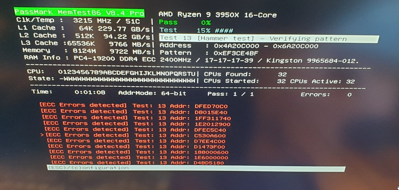
Although I’m very happy to hear that he managed to see reporting of ECC Errors on the Asrock Rack X470D4U when using a Ryzen 3950 (Zen 2), I’m also confused and puzzled to what this means for my failing experiences to achieve the same…
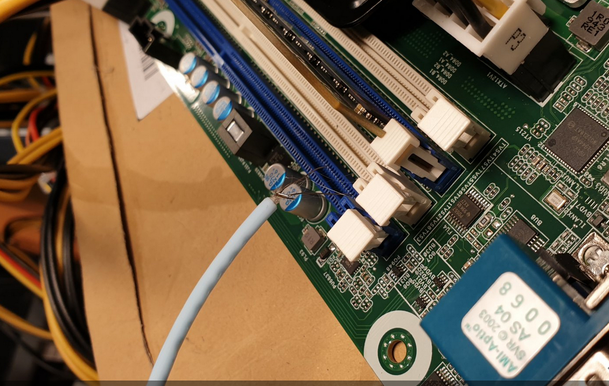
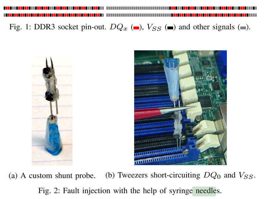
Causing memory errors by shorting pins of memory modules
Firstly I did some research on this “Triggering memory errors using ‘needles’ or wires”-approach, which Diversity has used. I didn’t look into this method yet, as it seemed too risky and I didn’t want to damage or degrade any of my hardware.
So in short, you’re connecting a data-pin with a ground-pin, so that the current on the data-pin “flows away” into the ground-pin and this “flips a bit”. When using the correct pins and not accidently shorting anything wrong, this should actually be “reasonably safe” to do I think… (please correct me if I’m wrong )
Why is this causing single-bit errors and not multi-bit errors? I THINK because every “clock tick” data is pulled from each data-pin of the memory module. So if you change only the “result” of 1 pin, you get a maximum 1 bit flipped per “clock tick”, which ECC can then correct. (not sure though)
This paper is already a bit older and was using DDR3. The ‘AMD-1’ configuration they are talking about (where interleaving is making things complicated) is an ‘AMD Opteron 6376 (Bulldozer (15h))’.
As far as I understand, the extra complexity of “interleaving”, that happens on the Opteron system, is only applicable on Ryzen, when using Dual Rank memory. As Diversity was using a single 8GB module, I suppose he only has single rank memory, so wasn’t confronted with the “interleaving-complexity”. However, if I would try this with my 16GB modules, I would be confronted with this extra complexity, because ?all? 16GB modules are dual rank…
I concluded this from this article (but I could misinterpreting things!):
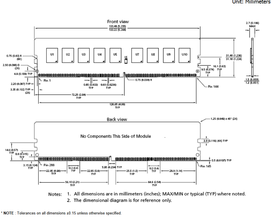
As the paper was for DDR3, you of course need find the pin layout of DDR4, before you can apply it on Ryzen. Following datasheet has pretty clear pin layout of unregistered ECC DDR4 module:
On page 6, 7 and 8 you can see the description per pin and on page 17 you can see a picture of where those pin numbers are on the memory module. I suppose all VSS-pins are ground pins and DQ+number pins are data pins. So if we follow the example of the paper and short DQ0 with a VSS, the corresponds to shorting pin-4 (VSS) with pin-5 (DQ0). But I guess shorting pin-2 (VSS) with pin-3 (DQ4) could work equally fine.
This should help us “understand” a bit better what Diversity has done and how to “safely” reproduce it.
The results from Diversity
I was in contact with Diversity and have some more details on his testing (all pictures in this “chapter” are from Diversity himself). Diversity used the following video: https://www.youtube.com/watch?v=_npcmCxH2Ig. Instead of needles and tweezers, he used a thin wire, as in the picture below.
As you know, I also tried triggering reporting of corrected memory errors. I tried this by overclocking / undervolting the memory to the point where it is on the edge of stability. This edge is very “thin”, can be hard to reach and can result in the following scenarios in my understanding:
Not unstable enough, so no errors at all
Only just unstable enough, so that single-bit error occurs only sometimes when stressing the memory enough. These will then be corrected by ECC and will not cause faults or crashes.
A little more unstable, so that single-bit errors occur a bit more often and less stress is required on the memory to achieve this. But also (uncorrected) multi-bit errors can occur sometimes, which could cause faults / crashes.
Even a little bit more unstable, so that mostly multi-bit errors occur when stressing the memory and single bit errors might be rare. This also makes the system more prone to faults and crashes.
Even more unstable, so the multi-bit errors occur even when hardly stressing the memory at all. This makes the system very unstable and probably will not be able to boot into OS all the time.
Too unstable, so that it doesn’t boot at all.
Both scenario 2) and 3) are “good enough” for testing reporting of corrected memory errors. Perhaps even scenario 4), if you’re lucky…
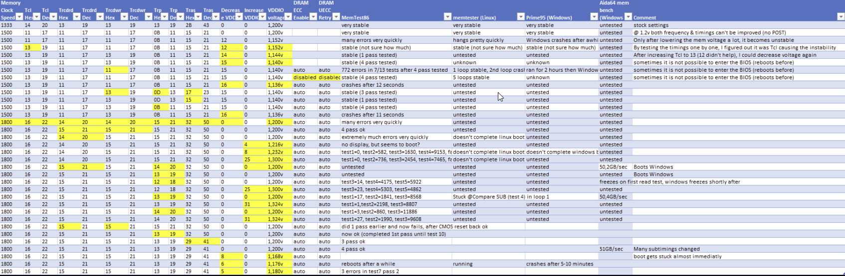
During all my testing I tried 100+ possible memory settings, using all kinds of frequencies, timings and voltages, of which 10-30 were potentially in scenario 2) or 3). I “PARTLY” kept track of all testing in the below (incomplete) Excel:
This convinced me that I should have at least once been in scenario 2) or 3), where I should have seen corrected errors (but didn’t). That is why I concluded that it didn’t work and I contacted Asrock Rack and AMD to work on this.
Conclusions / Questions / Concerns
Now what does all of this means? Does this mean that I never reached scenario 2) or 3)? Does it mean scenario 2) and 3) are almost impossible to reach using the methods I tried? Or does it mean that Diversity perhaps triggered a different kind of memory error? I’m not sure and I hope someone can clarify…
I know there is error correction and reporting happening on many layers in a modern computer. As far as I know, there are these:
Inside the memory modules itself (only when you have ECC modules). The memory module then has an extra chip on the module to store checksums. I think this works similar to RAID5 for HDDs. So that a memory error is detected and corrected in the module itself, even before it exits the memory module.
On the way from the memory module to the memory controller on the CPU (databus). Error detecting / correcting / reporting for these kinds of errors are handled by the memory controller in the CPU, so ECC memory isn’t even required to make this work.
Inside the CPU data is also transfered between L1/L2/L3 caches and the CPU. Also there Error detecting / correcting / reporting is possible I think.
All of these might look confusingly similar when reported to the OS, but I do think they are often reported in a slightly different manner. I’ve seen reports where the CPU cache (L1/L2/L3) was clearly mentioned when reporting a corrected error for example, but I’m not sure what the exact difference between reports of 1) and 2) would be.
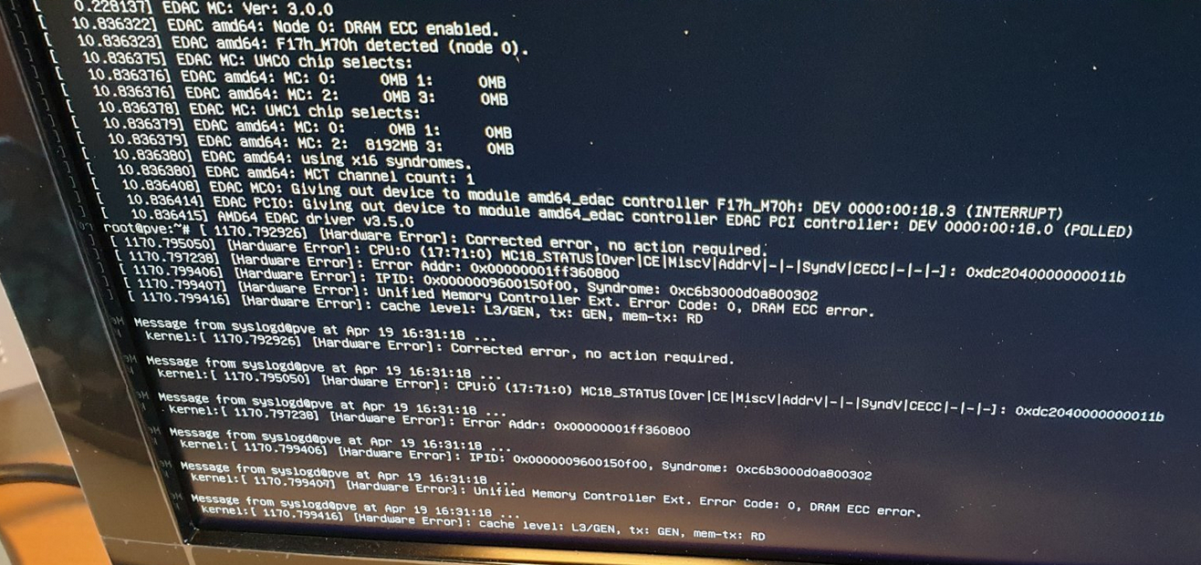
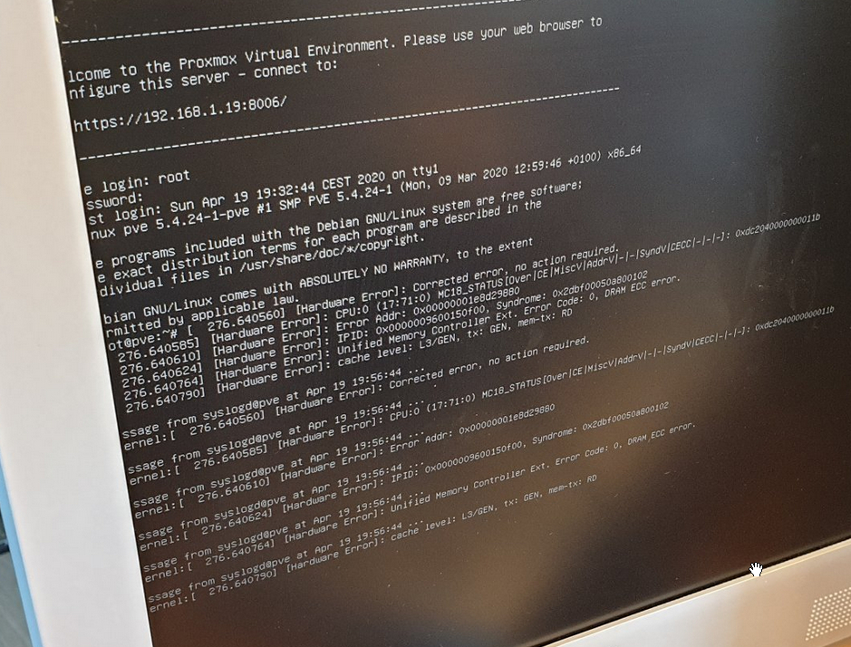
In Proxmox screenshots I do read things like “Unified Memory Controller…” and “Cache level: L3/GEN…”, but again, I’m not entirely sure if these mean that the errors are in 2) or 3) instead of 1)…
Diversity is draining the current from a data-pin “outside” of the memory module, but I still see 2 possibilities of what’s happening:
1) The drain on the data-pin is pulling the current away also inside the memory module itself, where the memory module detects the error, corrects and reports it.
2) The drain on the data-pin only happens after the memory module has done its checks and the error is only detected on the databus and corrected / reported there (so not by the ECC functionality of the memory module).
To know which scenario is happening, we could:
try to find someone with knowledge on exactly how each type of error is reported and who can exactly identify what is being reported
perhaps using a non-ECC single-rank module also reports the same kind of ECC errors, which would proof it is happening on the databus.
perhaps someone with more (I don’t have any actually) electrical engineering knowledge can also say something more meaningful than myself?
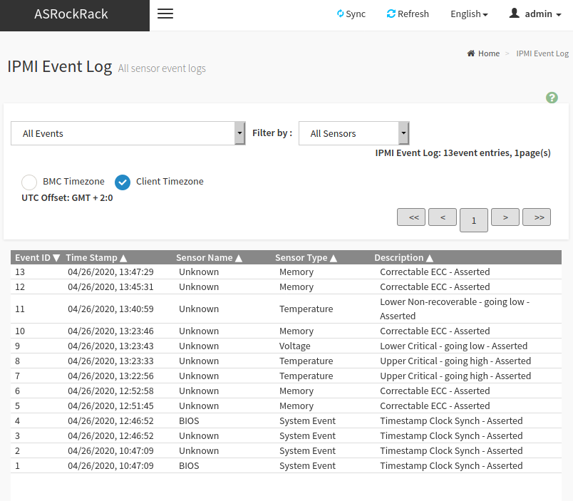
Diversity did mention that his IPMI log was still empty after getting those errors. So there the motherboard / IPMI is certainly missing some required functionality.
Edit:
As Tenrag correctly commented, the memory modules don’t do “on-module-error-detection-and-correction” because they’re missing components to do so. So even when using ECC memory, it is the memory controller on the CPU, using the extra parity chip on the memory modules, that detects / corrects / reports the memory errors.
Also according to Tenrag, the EDAC output does point to actual memory errors being detected (-> DRAM ECC error) and not data bus (infinity fabric) errors (-> link error).
Finally MasterPhi also correctly questioned if I had disabled PFEH during my testing and I did not actually, since I only discovered this BIOS setting very late in my testing (I only did my final testing with PFEH disabled).
So I may need to do some more testing with PFEH disabled…
I initially wanted to try out 3.33 for the agesa version that fixes pci pastthrough. I couldnt keep my machine up for more than 5mins.
I then tried to flash back 3.30 had instability where it was functioning perfectly for the past 3months. So at a last ditch i flashed 3.20 and it’s been running ok for the past 9 hrs. I’m running centos8/fedoraserver31.
@Mastakilla Thank you, great work, I remember reading this article about DDR3 and were wondering how long before someone would do this for DDR4.
Now I wonder how long before someone starts selling some ‘dimm risers’ with an ‘inject error’ button…
AFAIK nothing is checked on the memory module itself. Both data and parity is transferred to the memory controller and checked there.
If it was done on the memory dimm then we would see one of following 2 things on the PCB:
8 DRAM chips with increased capacity/integrated error correcting logic inside of each.
9 DRAM chips + a separate chip for the error correction
If you take a look at your ECC UDIMMs you will find neither. There are only 9 regular DRAM chips and a bunch of passive SMD components.
About the screen captures: if you go to the IPMI and launch a KVM you can make screenshots of the output. So you do not have to take pictures of the screen.
And you can also take advantage of the 2 integrated serial ports for easily copyable outputs:
there is a traditional RS-232 connector
(more convenient) Seial-Over-Lan.
You can enable both in the BIOS in the ‘Super IO Configuration’ menu
And you can also redirect the boot process itself - in the ‘Serial Port Console Redirection’ BIOS menu (You will be able to change BIOS options from the command line on the remote machine without launching full KVM)
I experienced the same with my ‘seemingly faulty’ board
Yes, or there are multiple error reporting protocols. And Ryzen simply does not implement all of them. But that’s just me speculating.
So If I understand correctly something like [Hardware Error]: cache level: L3/GEN
means just that the error was detected while loading the data into L3 Cache. Which is expected since the memory is usually loaded into the highest level cache first.
Thanks, Good point about the memory modules missing components to handle the error detection themselves! That makes totally sense…
About the screenshots: I know… They are screenshots by Diversity. I didn’t try serial-over-lan yet though…
Not sure what you mean by “error reporting protocols” and Ryzen not implementing them all. If an OS like Linux can detect “Hardware Errors”, then the IPMI should be able to do the same, right? And it seems only logical to me to also expect this from the IPMI, no?
Hehe… c code… That has been awhile for me… Will try to look into this file a bit better…
Were you able to find anything in there that confirms that Diversity his errors are certainly errors from the memory modules ECC logic (and not from the infinity fabric or CPU cache)?
All my testing was done with PFEH enabled, except for my very last couple tests… (after discovering this BIOS setting)
I’ll check with Diversity if he had PFEH disabled during his tests. If he had, then I may need to do some more testing with PFEH handling and then maybe most of my previous testing is “invalid”…
Yes, that would be logical but I do not know how exactly those errors are supposed to be detected/delivered, maybe the CPU reports those errors in multiple ways.
For example take a look at the IPMI specification:
In chapter 16.1:
The figure shows a BMC with a shared system messaging interface where Event Messages can be delivered from
either BIOS, SMS (system management software / OS), or an SMI Handler, and an IPMB interface and through
which it can receive Event Messages from the Intelligent Platform Management bus. The BMC can also generate
‘internal’ Event Messages.
TL;DR: there are multiple ways that events can get into the IPMI log.
I am trying to say that without some more detailed knowledge it can be misleading to suggest that IPMI is seeing errors but does not report them.
Conspiracy theory: Maybe it is IPMI, maybe AMD forced Asrock to remove some features to force market segmentation. Maybe that is why when we ask Asrock about ECC we always get the same copy-paste answer saying that ‘AM4 does not support ECC error reporting function’. For now we just can’t be sure where exactly is the missing part.
From what I can tell after reading the source: Seeing this in dmesg is a confirmation for me: [Hardware Error]: Unified Memory Controller Ext. Error Code: 0, DRAM ECC error.
Those strings would be different if it was infinity fabric or cache itself.
Example 1:
Memory controller errors are on ’ SMCA_UMC’ bus, which points to “Unified Memory Controller” name and points to ‘smca_umc_mce_desc’ string array:
NOTE : These pre-defined events will likely not produce “accurate” SEL records for a particular system because they will not be correctly tied to a valid sensor number, but they are sufficient to verify correct operation of the SEL.
It is possible to inject errors to ‘real’ sensors using ‘event’ command but I can’t find a way to inject ECC error. I was able to inject the voltage and temp events (on the screenshot above).
I also checked ‘event’ command on my other Intel based Supermicro board and the result is the same. I can’t find a way to inject ECC errors. So I do not think that my inability to inject ECC errors here means anything in relation to Ryzen.
Hey All,
I think I did a dumb and need a sanity check if anyone is willing.
I purchased the X470D4U as well as a 3950X for it. I’m moving off of an old eBay’d system that I was running unRAID on. I got the new components assembled and tested out. Put them into my system today and am running into some issues.
I have 3 PCIe devices I’m reusing from the old system:
Nvidia Quadro P2000
Mellanox ConnectX-2 dual SFP+ card
LSI SAS9211-8i
I’m able to get the system booted up with the HBA and network adapter but when I add the Quadro into the mix it’s a no-go. The system goes into a loop of giving me the SAS controller and ConnectX-2 information screens but then but then dumps back to the ASRockRack logo and starts over again. I’ve not gotten it to proceed to the point where the system tries to boot into unRAID or, oddly enough, even though I catch an F2 to get into the BIOS it hasn’t wanted to load into it for me
I’m hoping I didn’t make some egregious error when planning things out and mis-count the number of PCIe lanes I had available or something.
I’ve tried with keeping the Quadro in PCIe 6 and swapping the HBA and NIC between 5 and 4 (as I type this I’m pretty certain I haven’t tried putting the GPU in slot 4 but it’s been a long day…)
If my notes serve me well; I also found that if I remove the GPU and leave the HBA and NIC occupying slots 6 and 5, doesn’t matter the order, both of those devices are recognized and work correctly. However, if I put either of the cards in slot PCIe 4 it is recognized in the system inventory of the management UI but when booting into unRAID it complains of either not seeing the network interface or any of my drives (big oof).
All PCIe card were in working condition when they were pulled from the old system, I take precautions with regard to static discharge, etc
So I guess at the end of all this I’m wondering if something is wrong with the board or if quarantine brain got me doing stupid things.
 )
)