Just stumbled across this SemiAccurate "article":
https://semiaccurate.com/2016/05/22/38688/
This is what the most common guess it to how Zen will be: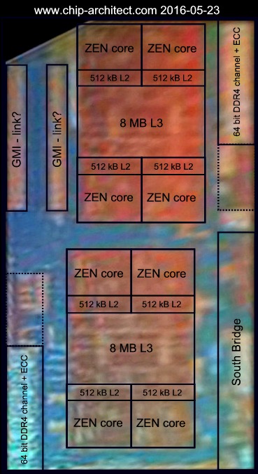
The image looks so bad because this is where it came from:
Just stumbled across this SemiAccurate "article":
https://semiaccurate.com/2016/05/22/38688/
This is what the most common guess it to how Zen will be:
The image looks so bad because this is where it came from:
odd looks.
integrated south-bridge ? >_> is this really zen?
Doesn't look like any die shot I've ever seen. If those numbers are correct though, then zen looks nice.
It kinda looks like Jaguar (AMDs console processor) with the two seperate core arrays.
If that is 8 cores (2 groups with 4 cores) then 16 cores are not too far out.
That could really be a zoomed out blue potato with random red(ish) dots.
A bit, expect it seems to be split into two sections. Hopefully there are 8 big cores.
On the slide, you can see that there is some gap between the L2 caches. So I suppose it is not the shared L2 nonsense anymore.
looks very rectangular.
If you look at Intel's dies, they're just as rectangular.
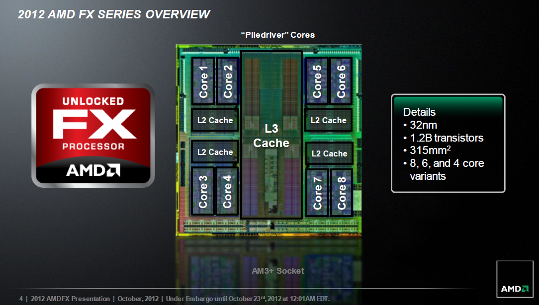
One of the biggest faults with Bulldozer is the shared L2. 512kB is less per core than what Bulldozer had (was sharing 2MB between two cores) but twice the L3, which was another concern with Bulldozer. Combine the improved cache layout with SMT (ie hyperthreading), smaller node (which means better performance and higher clocks naturally), and architectural improvements, and we have some serious improvement over the 8350. The new socket should really help things out too. I am pretty excited to see benchmarks of this thing come out. The current word on the street is that it is close to 5960X levels of performance. I find that hard to believe, but would be very interested if it were true. Of course, I don't expect them to try to price it anywhere near that high, but it would coincide with what Lisa Su was saying about getting back in the performance game.
Also, AMD seems very precise about their wording with the performance levels as of late. For GPUs, they said that Polaris is mainstream, not high end or enthusiast. This coincides with the recent leaks that it will be the 480, not the 490 or the Fury replacement. Now, from what I know, AMD is calling Summit Ridge (particularly the 8core Zen part) an "enthusiast" cpu. Intel markets their x99 platform as "enthusiast" as well. Makes me think that they have been aiming for x99 levels of performance with Zen from the get go.
It actually came from this image:
That image came from the bottom left of the slide.
And in the slide it's about 1/10 the size. This is the high resolution version that the crop and reshape came from. There is the standalone die shot image, and the marketing slide. They are separate.
tl;dr I think that the L2 is 1MB per core and that the die size is roughly 140mm^2 at 14nm.
I am trying to figure out the die size of this chip, and I can't come to a sensible number. I used the L2 cache as a way to compare the die shot here to the one of Bulldozer. If this is actually 512kB each and those are actually comparable (ie surface area and number of kB is linear relationship), then we get a die size for this chip of 138mm^2 on a 32nm node (which is what Piledriver is). Shrink that by over 1/2 as the density increases roughly 2x going from 28nm to 14nm based on the gpu rumors and all, and you are looking at a die size well under 100mm^2. Simply not sensible. So there are a few things that could be wrong here. It could be that there is more than 512kB or L2 here which is what I think it is. IT could be the the surface area to kB ratio is different between the two dies which I doubt is a huge issue. This could not actually be Summit Ridge which I doubt as well considering that the first Zen cpu available will be the 8350 replacement in October, so that is likely what we are looking at. If we assume that it is 1MB of L2 cache, then we are looking at a little less than 150mm^2 die on 14nm which is much more believable considering that Skylake (also 14nm though different process) is at 123mm^2.
EDIT: This guy agrees.
Rather fitting that there is a WCCFTech watermark on that image, isn't it? Guys this is a marketing photo, and is in no way necessarily representative of the actual die shot. Lets wait till official shots are released before we go running around yelling "what ifs"...
Just looking at the official slides, the core layout fits.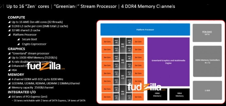
Something interesting that I calculated. IF I am right about the die size, then they can get 2.5x more chips per wafer compared to the 8350. I could be totally off base with that though.
Here is the full WCCF Tech Article if anyone cares. Fairly in depth. Whether or not it is accurate is anyone's guess but the claims don't seem too far fetched.
Its hard to see what is really in that die from that picture, but I believe the labeling is wrong. I think this is a quad core and what is labeled as a Zen Core is actually a thread core. The area labeled as L2 is actually L1, the area labeled as L3 is actually L2. The areas labeled as "GMI - Link ?" are actually the interfaces to the L3 and the area between those two areas is the actual L3 static RAM. It just makes more sense to me that way. Having two separate NUMA cores on the same die without cache coherency doesn't make sense to me which is why I believe the labeling is incorrect.