If the CPU doesn’t fit you must acquit.
3 Likes
Or use a hammer 
1 Like
Or “CPU Installation Tool” as its known if you are watching Verge videos.
2 Likes
I guess you could read that they cant make that memory thing 7nm?
and if this is the future, maybe CPU’s will also get that HBM collar
Finding this whole chiplet thing amusing as I did before write that to describe GPU core counts, and guess now I’ll demote them to be chiplings instead
Shhhhh! Equifax might hear you!
The I/O is simply the same 14nm process that’s been in use since 2015. It’s mature and cost effective, and no extra tooling or manufacturing ramp-up is required to print new designs on it. There are likely a few different I/O configurations being produced on that process and I’d bet that all of them combined cost less to make than a single 7nm chiplet at this point in time.
Okay, so using the socket information from this page
and the Anandtech photograph and some perspective magic I get the following measuerments:
core die:    7.1(2) mm x 10.1(3) mm
io die:     15.4(5) mm x 28.2(7) mm
take these measurements with a huge grain of salt, there may be systematic errors, the image resolution is not particularly high and I don’t know focal length and crop that was used to arrive at that image. Also I have systematically smaller values than this guy on reddit (although I don’t know his methodology):
If it fits it wil be thight, but the rumors wil flow wide and numerous the coming time. And some one wil go and count pixels and we wil know.
1 Like
Well, unless we get a better picture I don’t think we can get much better numbers, there is not a whole lot you can do with that image. I did my best.
There are enough people there with good dslr’s just wait. 
1 Like
It seems like this is the full event on video, from AMD themselves:
still 360p lol 
5 Likes
Package comparison
Epyc 7601 vs Rome X

Approximate Rome Chip Sizes
Single Chiplet: ~8.2(2)mm x ~9.5(3)mm (~78mm2 )
Uncore/IO ~ 17.0(3)mm x 27.7(3)mm (~470mm2)
Summit Ridge ~ 22.06mm x 9.66mm (213mm2 )
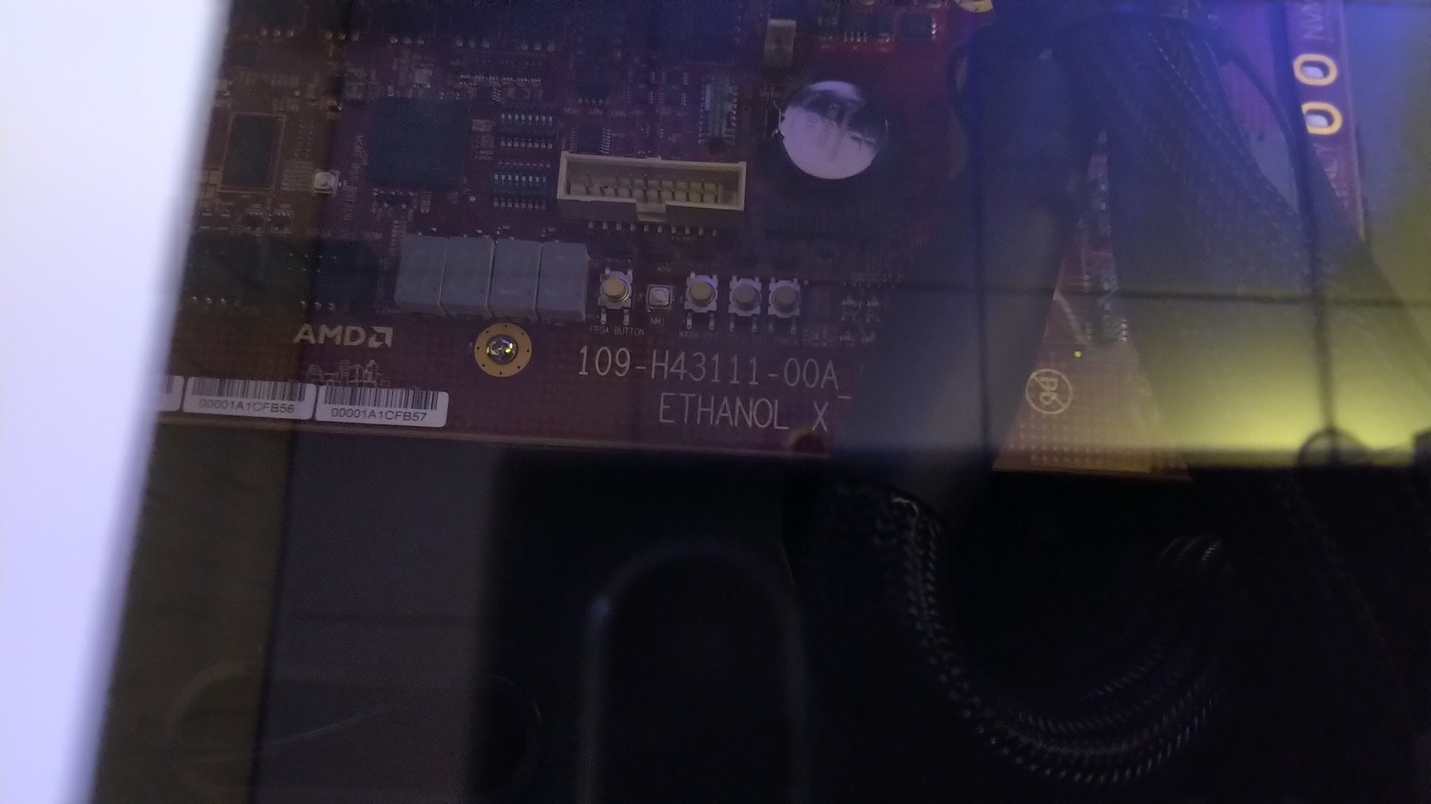
Ethanol X mainboard,
pic by Ian Cutress
4 Likes
Are these now the official numbers or have you also got those from a picture?
vega (as whole arch) has 1:2 ratio so
(INT16) FP16 will be 29.4TFlops; (FP16 tho hasn’t been used a lot, mainly in gaming)
It has limited support for INT8 *QSAD; offering only 58.8TFlops
(so INT4 should be 117.6TOPs)
‘Tensor’ cores are just market naming for INT4 | 8.
// Note: current Vega(10) 14nm, already has exposed INT8 QSAD in ROCm. New part here is likely INT4 which hasn’t been exposed yet.
Note 2: You would typically use FP16 for raytracing if you aren’t concerned about proper calculations; INT4-8 would be typically used for image processing - like filling holes for missed traces - aka nv ai for pixel approximation for rtx tracing)
No these are approximate based on package comparison vs Epyc 7601.
I updated it again.
There is a tiny bit of filler included in that measurement perhaps.
But the total area is close to what AMD said of just around 1000 mm2 total 
1 Like
Thanks!
It’s close to the numbers I got, so I guess we are in the right ballpark. What was your base image?
Would this PCIe 4.0 100gb/s whatever enable using pcie / m.2 ssd as vram instead of ram, for artsy stuffs?
I simply adjusted the image to fit the Epyc Interposer PCB size of 58.5mm along the short edge.
Btw Socket SP3 (4094) is 58.5 mm × 75.4 mm with 0.05mm margin allowed on the edge.
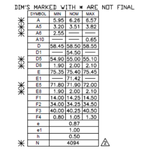
Values D & E
1 Like

aaah good times.
1 Like
8 noticed because of another topic, but AMD have AMD Rays for at least the wx line of cards. So like most things nvidia nothing new and oversold.
1 Like