AMD struck out a new wafer supply agreement with GloFo, looks like AMD got a fair deal considering glofo axed their 7nm.
2 Likes
Highlights
while the latest amendment sets purchase targets through 2021, the overall WSA itself will still run through March 1, 2024.
AMD has slated all of their currently-announced leading-edge 7nm CPUs and GPUs to use TSMC’s 7nm process, and AMD is further free to tap Samsung as well if they desire.
… if AMD fails to meet the annual wafer purchase target for 2019, 2020, and 2021, it will have to pay GlobalFoundries “a portion of the difference” between the actual wafer purchases and the planned target for that year. While this is not exactly a take-or-pay agreement that AMD used to have with GlobalFoundries several years ago, it will still have to use/sell 12LP and 14LPP chips in high volumes in a bid not to pay charges to its partner.
The statement by AMD reads as follows:
… GF continues to be a long-term strategic partner to AMD for the 12nm node and above and the amendment establishes purchase commitments and pricing at 12nm and above for the years 2019 through 2021. The amendment provides AMD full flexibility for wafer purchases from any foundry at the 7nm node and beyond without any one-time payments or royalties.
Thoughts
I wonder if the comment about Samsung is just for context of the other major players, or is AMD actually considering them?
Those last three years of the WSA, 2022, 2023, 2024, what is AMD on the hook for? For the moment, AMD can use GF wafers for IO dies, but by 2024, will 12nm still be good enough for IO dies? If not, could the supply be used for chipsets?
Could AMD force GF to license Samsung’s process for 7nm or below if necessary?
Die shot of the Exynos 9820 made on the Samsung 8nm node.
As expected it’s considerably less dense than TSMC 7nm.
It comes in at 127mm².
6 Likes
I got asked a while back about how to learn more about semiconductors and how they are made, I threw together a list and I thought I might as well share it here too for anyone interested.
Must read article
https://www.anandtech.com/show/8223/an-introduction-to-semiconductor-physics-technology-and-industry
Step by step, by Hitachi
https://www.hitachi-hightech.com/global/products/device/semiconductor/process.html
Simple educational video
Advanced educational video (credit @redgek)
Wikipedia page
Step by step, by samsung.
A real good site for this stuff is https://www.realworldtech.com
Some architectural talks
6 Likes
It is hard not to see a world where phone CPU’s are far ahead of intel’s best and AMD’s outsourced are. It a bleak world when mobile and laptop distinctly beats desktop.
I think apple are pivoting already 
Without a war it’s all about money and all the money is in kids and phones.
That’s definitely how I see things going for PCs too.
However, as people move back toward teletype terminals er, thin clients and webapps, there is also demand for, and money in, server hardware.
To go off-topic for a bit, this is part of why I gush about Talos II in the Power Architecture thread; while companies are happy to lock down and limit what they sell to the unwashed masses, they want to keep their own hardware as open as possible.
For example,
if you look at Google’s activity, I think you can really see a good idea of the future we’re heading for:
-
On the server side, they support a bunch of open-source software everywhere. You see Google and other large companies involved in Open Compute Project, OpenPOWER, LinuxBoot, all projects aimed at increasing owner-control.
-
On the consumer side, Google pushes for devices dependent on
mainframeer, cloud services, and which are increasingly locked down and proprietary if possible. Google Fuchsia seems like another step in this appliance-ification direction; even if its opensource, it make porting a desktop OS like Linux more difficult.
The only way I see honest-to-goodness desktops surviving is as an extension of server hardware, everything else will be reduced to a phone/tablet or IoT “appliance” that is locked down like iOS or Windows S.
Older article I found, but it’s giving my brain a melt:
https://www.nextplatform.com/2019/02/11/giving-waferscale-processors-another-shot/
It talks about how not needing to package dies separately would be better, talks up waferscale integration (WSI) as better than Intel EMIB and TSMC CoWoS, but then describes a silicon interposer? Am I missing something, or is the ‘revolution’ here merely that of using full wafer’s worth of interposer rather than a smaller portion?
How would you even socket a 300 mm WSI module in a mainboard?
Slot processors
1 Like
If you are going to do that, might as well make the case out of an old FOUP. Then your server room would just look like part of a fab.
Meanwhile 3 months later…
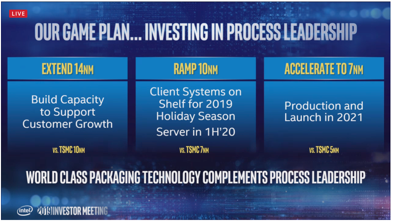
We are back at 14+++(++++…) Still no sign of regular supply or anything in volume at 10nm from Intel.
1 Like
Gamers Nexus’ recent news summary mentioned that Intel is reporting better progress on 10nm, and is “on track to have volume client systems on shelves for the holiday selling season” according to the earnings call. Still notebooks and no desktop parts though, by the sounds of it. GN also mentioned that Samsung has announced large investment in logic chips specifically:
I realize I’m pretty clearly obsessed with IBM’s POWER line of chips, so my perspective is a bit biased, but I can’t help wondering if IBM’s use of Samsung for POWER10 is part of the reason for this growth.
Their mainframe chips will also be moving to Samsung; not the next generation (z15), but the one after that (z16). I guess for mainframe customers, it’s worth it to use an entire product line (POWER10) as a pipe cleaner, to get accustomed to 7nm?
Question is, will IBM be using normal Samsung 7nm, or will they be getting a custom variant, like they did at 14nm with 14HP?
1 Like
Globalfoundries selling Fab 3E and 10
-
GF Fab 3E in Singapore is being sold to Vanguard, with equipment, staff, MEMS customers, and manufacturing IP as part of the sale. Sale completes on December 31, 2019.
-
GF Fab 10 in New York is being sold to ON Semiconductor. What’s interesting here is that this is a 14nm fab, and the one that IBM uses to manufacture their chips. I think it is because of this, that the sale sort-of happening now, but only truly completes in 2022 which is when IBM plans to be manufacturing POWER10 and z15 at Samsung on 7nm.
- https://www.anandtech.com/show/14254/globalfoundries-to-sell-300mm-new-york-fab-to-on-semiconductor
- https://www.bizjournals.com/albany/news/2019/04/22/globalfoundries-selling-east-fishkill-chip-fab.html
- https://www.it-zoom.de/dv-dialog/e/ibm-statement-zur-power-zukunft-22837/ (in German, but readable enough through Google Translate)
Rumors, Rumors. However if it pans out we could get a Zen2 and Zen2+ on 7nm. Then 5nm after that.
TSMC’s stated parameters for 5nm aren’t in line with IRDS’ 2017 figures. Transistor gate and interconnect pitch for the process are set as 48 and 30nm respectively; which is more in line with the parameters for 7nm.
I really don’t have the knowledge to make a good guess here, but this sounds like it’s a more of a 7nm+?
I’ve heard the mantra that Intel 10nm = TSMC 7nm, but for all other nodes, what are we really supposed to look at? Which transistor/interconnect pitch/width/height should we be comparing to get a rough sense of TSMC vs Samsung vs Intel?
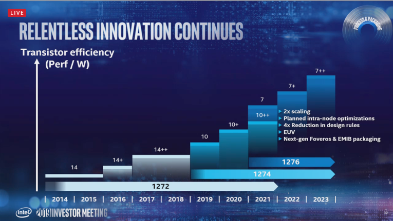
Intel got some updates
GPU first to hit 7nm
2 Likes
As seen above Intel is comparing their 10nm to TSMC 7nm,and their 7nm to TSMC 5nm.
The densities for Intel 10 vs TSMC 7 should at least be similar.
The next node adds EUVL to the mix.
Ice lake shipping in June.

10nm seemingly short lived, 7nm in 2021
Wikichip’s article has some diagrams of them putting memory physically on top of the compute silicon. I can’t fully grok it, but that means it belongs in this thread, right?
Samsung detailed their 3nm GAAFET process at their foundry forum
https://www.anandtech.com/show/14333/samsung-announces-3nm-gaa-mbcfet-pdk-version-01
3 Likes
I am reproducing what I posted in a couple places here. If it doesn’t seem fully in context, it is due to copy/paste from my prior post:
[QUOTE]10nm has some really aggressive UHP (Ultra High Power i presume) cell libraries, that sacrifice way more densitiy than 14nm++ (vs 14nm HD):

It remains to be seen when Intel finally manages to ship silicon using that process. If they do however, it should clock quite decently. The main question is of course when will that be ?
If I had to guess, I’d say, probably a year after the mobile Ice Lake releases (if no additional issues crop up)- Considering that Intel actually seems to ramp up 10nm now. $530M dollar loss for ramp-up at least means they are somewhat more serious of actually delivering something by the year-end.[/QUOTE]
This is a repost of my analysis on why Intel’s purported density means NOTHING in discussion of actually implemented density on chips:
Post 1 -
https://www.semiwiki.com/forum/content/6713-14nm-16nm-10nm-7nm-what-we-know-now.html
Post 2 -
So, I thought at first that the 66MTr/mm2 was from the estimated density for the Apple A12, which was floated around the time of its release. I was wrong. Here is the information to analyze density comparisons for process nodes to put them into context:
This is the list on approximate transistor densities with some information on context. (full source: https://www.techcenturion.com/7nm-10nm-14nm-fabrication ).
As you can see, when you compare Intel’s SRAM numbers, the only one provided, to TSMC’s HPC process, that is where the comparing 100.8 to 66.7MTr/mm2 comes from. But take notice that TSMC’s low power process for mobile chips is at 96.5MTr/mm2.
Now, let us examine an Anandtech chart looking at actual densities in final silicon:
https://www.anandtech.com/show/13687/qualcomm-snapdragon-8cx-wafer-on-7nm
Notice that for the companies that used the TSMC 7nm FF/FF+ node, Qualcomm reached to up to 94.6MTr/mm2, the HiSilicon Kirin reached 93.1MTr/mm2, and the Apple A12 Bionic reached 82.9MTr/mm2. Those are 98%, 96.5%, and 86%, respectively, of the theorized transistor density. That is pretty good.
But let’s examine what happens when we look at Intel’s 14nm process, with the theoretical density of 43.5MTr/mm2. Intel, with Skylake 4+2 achieved just 14.3MTr/mm2, or a 33% density compared to the theoretical value that Intel published.
Let’s look at AMD’s results. Using Samsung/GF 14nm process with a theoretical transistor density off 32.5MTr/mm2, they achieved an actual density of 25MTr/mm2, or 77% of the theorized density. That is pretty good.
So, assuming that the achieved density versus theoretical will be approximately the same, while AMD is using the HPC TSMC process rather than the more dense low power variant, you would take the 66.7MTr/mm2 * 0.77 (77%), which equals 51.3MTr/mm2.
Now it is time for Intel. So, taking the theoretical 100.8MTr/mm2 * 0.33 (33%), you get 33.3MTr/mm2, or roughly 18MTR/mm2 less dense than AMD.
Now, one reason to do less density is heat. By making it less dense, the neighboring transistors contribute less so that the heat density is lower which can allow for higher frequencies at the same temp as a denser chip with lower frequencies. This is part of where Intel gets their high frequency. But, with that, you also wind up with fewer transistors to contribute to doing the work. So, there is a theoretical IPC trade-off. This also isn’t comparing the final transistor count nor the die area, although those are provided in the table above. When doing that, you can see why I am very impressed with Intel’s engineers ability to design microarchitecture. They have great performance with about 60% of the density of a Ryzen chip, while achieving 25% more frequency, with the rest coming from IPC due to architectural design.
One should always show respect for achievements. AMD deserves respect for achieving the density that they have, Intel on microarchitecture. But to look at densities in a vacuum, especially theorized on SRAM instead of actual results achieved, is more than misleading.
Once you change to the HPC libraries on Intel’s process, you are not getting anywhere near that 100.8MTr/mm2. It’s impossible. Just like going to TSMC HPC node reduces the density from the mid 90s to 66MTr/mm2. That means Intel CAN NOT hit that density on their desktop and Xeon offerings.
Edit: Now that I have woken up more and am having a cup of coffee, let’s examine the theoretical max of Intel 14nm vs your two examples and look at Xeon density.
The theoretical maximum is 43.5MTr/mm^2. The two examples you gave, which likely do not include the HPC libraries, are 34.5 and 30. That is 79.3% and 69%, respectively, the maximum theoretical density published by Intel. If those were built on the 14nm++ process, with a theoretical max of 37.22MTr/mm^2, then they reach 92.7% and 80.6%, respectively, while noting that the “+” variants reduce the maximum theoretical density… That is on a neuromorphic chip and an FPGA chip, both of which still fall short of what mobile/phone arm chips achieve on density using the 7nm FF/FF+ design from TSMC as a matter of percentage.
Getting back to Xeons, some have suggested up to 15.xMTr/mm^2 on those, which is without the iGP, and still only gives about 35% of the theoretical density on 14nm (a little higher on the “+” process variants).
So, unless you can show Intel reaching near the theoretical limit on their HPC libraries and mainstream and server options like Xeons, you are arguing that when you use an entirely different architecture on Intel’s process, you can achieve higher densities, neither of which is above the 80% mark. I will agree there. But Intel is using density for marketing and misleading on being most dense in regards to their chips because of a theoretical SRAM density. In practice, the chips consumers are buying, whether the mainstream, HEDT, or server Xeon offerings, are much less dense than the theoretical limit.
Edit 2: Also, if you compare Intel’s UHP libraries, under their own theoretical chart, you have a max theoretical density of 67.18MTr/mm^2, compared to TSMC’s HPC 66.7MTr/mm^2. You could argue that the nearly 0.5MTr/mm^2 theoretical max density is better. But, there still are questions as to whether Intel will achieve a high enough density under that compared to those using the TSMC node.
3 Likes