Seeing the better density is nice. Now, I believe it was mentioned somewhere that due to AMD libraries, the density is only around double rather than higher theoretical limits. Don’t know if true or not, but have seen that in passing. But it is exciting and proof that TSMC 7nm is doing well!
Intel 7nm on track, according to themselves
https://www.anandtech.com/show/13683/intel-euvenabled-7nm-process-tech-is-on-track
1 Like
So, according to schedule means, 7nm in 2019. This is good. We’re going to see some real competition for the first time in a decade!
1 Like
According to intel a few months ago, for the past 3+ years 10nm has been fine.
1 Like
3 Likes
Official news on the POWER10 chips using Samsung’s 7 nm:
Wikichip also has an article if you want to read something less corporate:
2 Likes
Its interesting because what little I know about IBM’s mainframes is what I learnt since they bought redhat. A Phoronixs test a few months ago put these mainframe machines running containers on par with AMD, Intel.
So 7nm CPU’s will keep them on track with AMD and well Intel at the end of next year may be back as well.
At long last a look at Intel 10nm and cannon lake.
https://www.anandtech.com/show/13405/intel-10nm-cannon-lake-and-core-i3-8121u-deep-dive-review
2 Likes
Just finished reading the article, highly recommended if you’re interested in semiconductors and how Intel measures up to TSMC and Samsung (spoiler; they are very equal).
It also gladdens me to see that anandtech did exactly what I requested a while back
1 Like
Well. Sort of. In reality, TSMC is building chips the size of Vega and Epyc / 8 core Zepplin dies. And by all reports, getting better than expected yields, and talk of running at up to 5GHz.
Intel can barely shit out a dual core mobile APU, with a broken on-die GPU on it - running at sub 3Ghz.
Irrespective of whether or not the process is good when it works, intel’s process is so badly broken (in terms of manufacturing) that they can’t actually build anything in volume with it.
Yeah, Intels process is much less mature. We’ve known that for ages though.
Don’t know if this is relevant but:
https://www.anandtech.com/show/13904/asml-to-ship-30-euv-scanners-in-2019
Initially EUV scanners will be used for non-critical layers, but their use will be expanded at the 5 nm node in 2020 – 2021. TSMC says that virtually all customers that use its N7 fabrication process will also use its N5 technology for their next-gen chips.
According to ASML, one EUV layer requires one EUV step-and-scan system for every ~45,000 wafer starts per month.
I’d argue that it is likely MORE mature, in terms of time they’ve spent on it. It’s just broken by design (due to the number of steps required as i understand it there’s a huge opportunity for any step to fail and cause the entire process to be a failure), and TSMC isn’t.
I was thinking mature as in functionality.
They’ve got a shit node and should feel shitty.
Move on Intel. You’re missing the boat.
2 Likes
We’ll see once ice lake comes out at the end of this year.
No doubt TSMC is in the lead right now.
AMD struck out a new wafer supply agreement with GloFo, looks like AMD got a fair deal considering glofo axed their 7nm.
2 Likes
Highlights
while the latest amendment sets purchase targets through 2021, the overall WSA itself will still run through March 1, 2024.
AMD has slated all of their currently-announced leading-edge 7nm CPUs and GPUs to use TSMC’s 7nm process, and AMD is further free to tap Samsung as well if they desire.
… if AMD fails to meet the annual wafer purchase target for 2019, 2020, and 2021, it will have to pay GlobalFoundries “a portion of the difference” between the actual wafer purchases and the planned target for that year. While this is not exactly a take-or-pay agreement that AMD used to have with GlobalFoundries several years ago, it will still have to use/sell 12LP and 14LPP chips in high volumes in a bid not to pay charges to its partner.
The statement by AMD reads as follows:
… GF continues to be a long-term strategic partner to AMD for the 12nm node and above and the amendment establishes purchase commitments and pricing at 12nm and above for the years 2019 through 2021. The amendment provides AMD full flexibility for wafer purchases from any foundry at the 7nm node and beyond without any one-time payments or royalties.
Thoughts
I wonder if the comment about Samsung is just for context of the other major players, or is AMD actually considering them?
Those last three years of the WSA, 2022, 2023, 2024, what is AMD on the hook for? For the moment, AMD can use GF wafers for IO dies, but by 2024, will 12nm still be good enough for IO dies? If not, could the supply be used for chipsets?
Could AMD force GF to license Samsung’s process for 7nm or below if necessary?
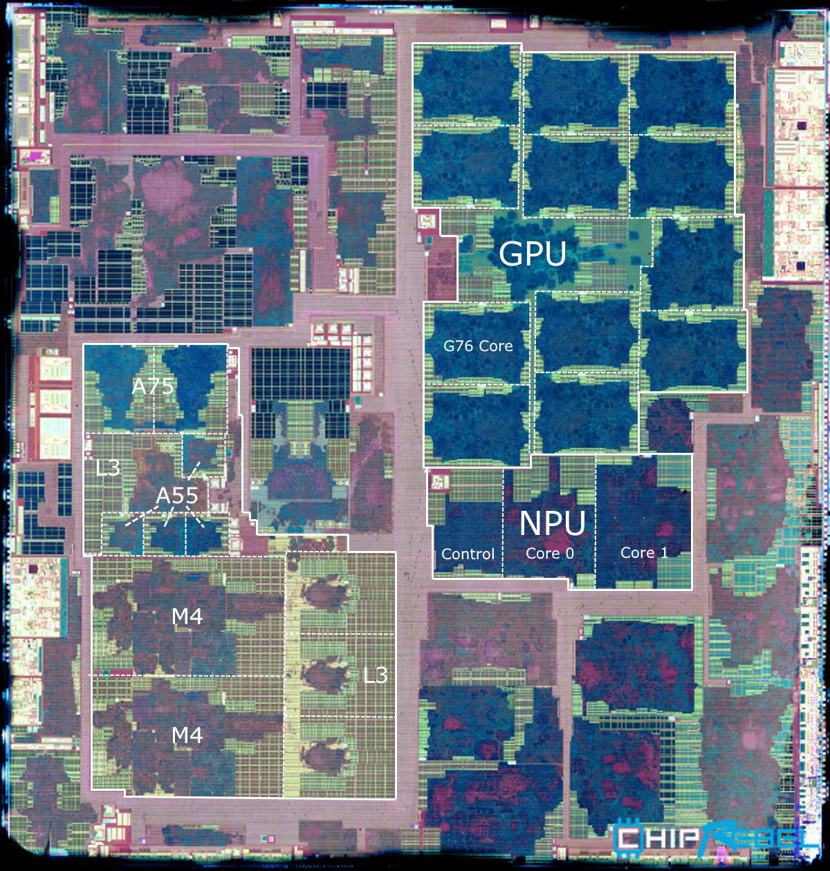
Die shot of the Exynos 9820 made on the Samsung 8nm node.
As expected it’s considerably less dense than TSMC 7nm.
It comes in at 127mm².
6 Likes
I got asked a while back about how to learn more about semiconductors and how they are made, I threw together a list and I thought I might as well share it here too for anyone interested.
Must read article
https://www.anandtech.com/show/8223/an-introduction-to-semiconductor-physics-technology-and-industry
Step by step, by Hitachi
https://www.hitachi-hightech.com/global/products/device/semiconductor/process.html
Simple educational video
Advanced educational video (credit @redgek)
Wikipedia page
Step by step, by samsung.
A real good site for this stuff is https://www.realworldtech.com
Some architectural talks
6 Likes
It is hard not to see a world where phone CPU’s are far ahead of intel’s best and AMD’s outsourced are. It a bleak world when mobile and laptop distinctly beats desktop.
I think apple are pivoting already 
Without a war it’s all about money and all the money is in kids and phones.