Someone needs to figure out how to adapt MI250 GPUs to PCIe

Yeah that’s correct. I do see it in lspci.

Interesting development worth noting for others: On my box with the PCIe OAM card, I can now enumerate the adapter with amdfwflash --list-devices after setting iomem=relaxed in my cmdline. (Thank you deepseek)

[sbin]# ./amdfwflash --list-devices
AMD Firmware Flash Tool Version 2.0.701.460-Public. Copyright© 2022-2025 Advanced Micro Devices, Inc. All rights reserved.

Detecting AMD GPU/APU. Please wait...
                                                                            IFWI      RMFW
                                                                            Update    Update
SNo BDF           DID ASIC      SPIROM          Size Test BIOS P/N          Available Available 
___ ____________ ____ _________ ___________ ________ ____ _________________ _________ _________
  0 0000:01:00.0 7408 MI200 (M) SST26VF016B 0x200000 Pass 113-D6520100-100         No        No

4 Likes

Great!

So, it is showing up as one single device. I think the second die is not visible with the adapter, right?

Can you see the device with rocminfo or rocm-smi?

lm5066 would make sense, it’s what I’m using for power control on mine - good balance of cost vs features.

No amdgpu driver still won’t load successfully just yet. Digging into that still.

I debugged mine at the bios level, EFI Shell has usually “pci” command which will let you see if its even enumerating.

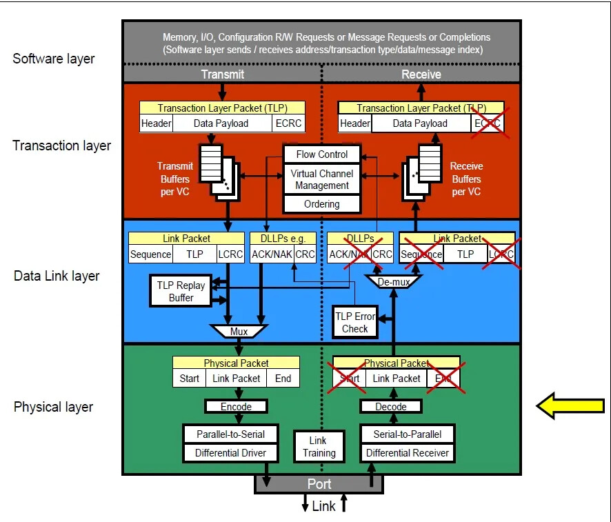
For me I then query the PCIe Root Port “pci 00 02 00 -i -b” and it shows its linked up but then had a protocol layer failure. Looking at the diagram before GREEN (Physical) is ok but something in the DLLP (Data Link Layer) is erroring but i cant tell what. Maybe it needs some specific feature in PCIe4 not in 3.

Im thinking something to do with 10-bit tags, large memory resizable BAR,

So I got a cheap Ryzen7 PCIe4 board and ran it at Gen4 (above 4G decode, resizable BAR) but still no pcie device id.

Reference Reading:

  1. Shane Colton: PCIe Deep Dive, Part 2: Stack and Efficiency
  2. Shane Colton: PCIe Deep Dive, Part 3: Scramblers, CRCs, and the Parallel LFSR
  3. Shane Colton: PCIe Deep Dive, Part 4: LTSSM
  4. Shane Colton: PCIe Deep Dive, Part 5: Flow Control
4 Likes

@gpufear to get lspci to work…

  • what motherboard & cpu combo?
  • which PCIe slot?
  • Any special BIOS settings you using?

For me;

  • Asrock Phantom Gaming4 + Ryzen7 3700X (Matisse PCIe Gen4) on PCIe Socket 1
  • Asrock Phantom Gaming4 + Ryzen7 5700X (Vermier PCIe Gen4) – TBD, pointless I think
  • Supermicro X10DAi + Xeon E5-2600v3/v4 – PCIe Gen3 x16 (Link up, but no pci ids)

I am sadly starting to think my card might be dead in some way, or the carrier is sending some broken signals of some type, or CPU combo is garbage and PCIe support is still lacking.

1 Like

I would imagine that if your card is working right this would be quite close to what I have been testing on (3900 + X570) and you’d see the device in lspci.

I’m inclined to agree, maybe there is something up with your card?

As for what I’m testing on now:

Supermicro H11Dsi-NT + 2x 7K62 - I moved to this after debugging to the point where the amdgpu driver was complaining that pcie atomic weren’t supported.


After moving over I’m not so sure that matters anymore, my attention is focused on the init routines in the amdgpu_asic_init path. The atombios spins waiting for some bits to be set, and I think it’s due to the GPU not being initialized already - the driver seems to rely on the module being active already.

Which makes good sense to me, why would we need a custom driver for an existing architecture?

But the driver path has been educational. Something needs to bring up the card before the driver can work with it.

And then I found the following in the HPE BMC image with the help of deepseek and psptool:

16MB image.bin — HPE EX235a node BIOS (BIOS 2.3.0, AGESA TrentoPI-SP3)
├─ Regions
│  ├─ 0x00000   padding/reserved
│  ├─ 0x20000   UEFI FV (small) + NVRAM at 0x21000
│  ├─ 0x120000  PSP Directory 0 ($PSP)
│  ├─ 0x3b0000  PSP Directory 2 ($BHD) — APCB/BIOS/PMU
│  ├─ 0x535000  PSP Directory 1 ($PL2)
│  ├─ 0x8c5000  PSP Directory 3 ($BL2)
│  └─ 0xd00000  Main UEFI FV (0x300000) — 200+ PEI modules
│
├─ CPU PSP firmware (PSPTool)
│  ├─ PSP_FW_BOOT_LOADER 0.25.0.37
│  ├─ Recovery Boot Loader
│  ├─ SMU_OFFCHIP_FW 0.43.29.0 (compressed)  ← WAFL AES encryption strings here (ARM/Thumb)
│  ├─ MP5_FW
│  ├─ DEBUG_UNLOCK / SEC_GASKET
│  ├─ DXIO PHY SRAM FW
│  └─ keys (AMD_PUBLIC_KEY, OEM key)
│
└─ MI200 GPU init — 4 UEFI modules in main FV
   ├─ AmdNbioBaseBaPei @0xd9c5e0
   │  ├─ AmdMi200Init
   │  ├─ Mi200PcieInitPei      (RootBridge/PCI bus)
   │  ├─ Mi200IOMMUInit        (reserve IOMMU bars)
   │  ├─ Mi200Wrapper/EngineConfigCallback
   │  ├─ NbioTopologyConfigureCallbackPpi
   │  └─ FabricAllocateMmio / GnbSetTomBA
   ├─ AmdSocSp3r4BaPei @0xdc81c0
   │  ├─ FabricSetMmioReg3     (RbNum ↔ DstFabricID ↔ MMIO pair)
   │  ├─ APOB handling (AmdPspApobLibConstructor)
   │  └─ PspBarInitEarlyV2
   ├─ WorkloadProfileBaPei @0xdf9138
   │  └─ PcdxGMIForceLinkWidth (force GMI link width)
   └─ CrayEarlyErrorCheck @0xf283a0
      └─ "GPU %d GMI/WAFL link training" error log (JSON format)

So it seems like the bring-up code lives in that image: the BMC/uefi image appears responsible for module startup.

6 Likes

@bitbashers regarding not showing up in lspci: I have been experimenting with power cycling the 48v supply at different times. When are you applying power to the card?

P12V1 and P12V2 are not connected to the internal wiring of the mi250x chip, and are all floating pins.

Is that a UEFI driver? Can you load it with UEFI shell?

This is extremely interesting to me. I am currently using MI210 GPUs for my plasma physics calculations and would absolutely love to run a single MI250. The G242-Z11 server that I am using now breaks out the PCIe 4.0 x16 onto daughter cards with MCIO 8i. If anyone comes up with a solution to run the MI250 off of MCIO I would happily pay for a solution and I could help engineer the final packaging, power delivery, and cooling. I really would like to be able to run one or two MI250 GPUs and I can’t support or justify a full 8 GPU server with my application.

The single PCIe OAM card seems to hide the required i2c interface from the host, unless there’s some (custom firmware?) work to make an i2c bridge possible on those cards I think my investigation there is blocked.

I have nothing of note to contribute yet, but, you have my sword.

I just reached the point in my “homelab” where I’m realizing the need for more. I’ve been sourcing barebones as-4124gq-tnmi (for less than $30k) to no avail other than sketch listings on Alibaba - and when searching for how to convert the UBB to PCIe I found this thread.

You all have made some insane progress in 3 months. I’ll chime back in once I have components to experiment with.

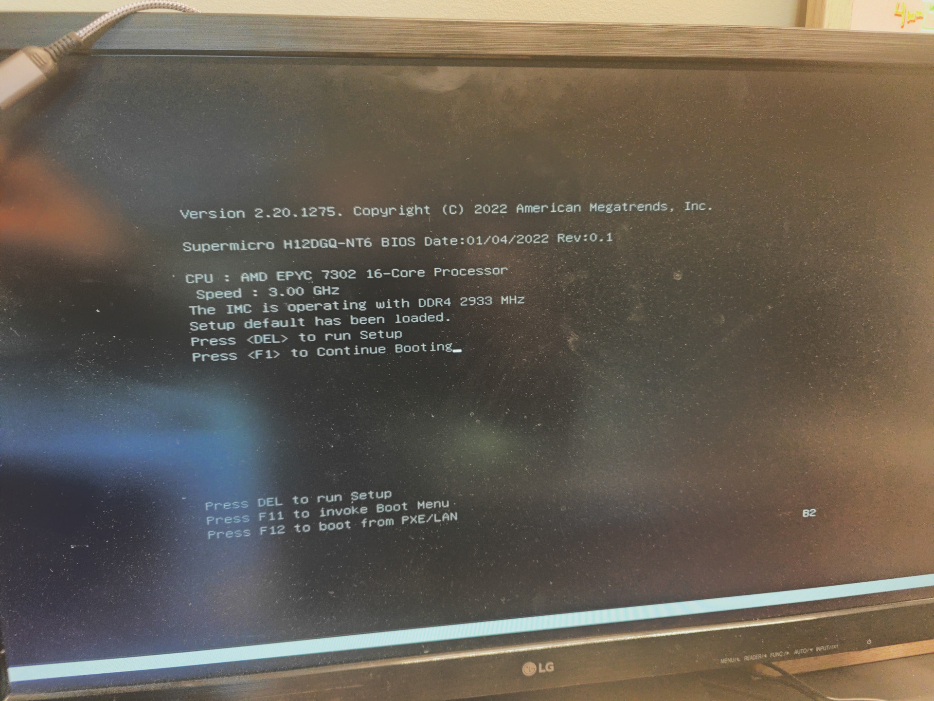
After a bunch of testing I’m pretty certain my H12DGQ-NT6 is DOA. BMC doesn’t come up, power button flashes yellow, PSUs flash green.

Considering my options. ASRock Rack ROME2D32GM-2T seems a possible way forward.

2 Likes

After some persistence and several CMOS clears

9 Likes

:open_mouth:

This is incredible work kudos to everyone involved! I’m fighting the strongest urge to dive in right now, knowing full well I’d get completely lost in the rabbit hole until I mastered it. Trying my best to finish my current projects first, but honestly, this is just phenomenal.

i fell in the rabbit hole :slight_smile:

I’ve been working on getting MI250/MI250X OAM modules running on standalone PCIe carriers.

After reverse-engineering both the module SPI image and the Supermicro H12DGQ-NT6 BMC firmware, we now have a much clearer picture of the module’s boot path and what the host/platform is expected to provide.

Anything marked [VERIFIED] below was checked byte-level against the module SPI dump and/or BMC image.

Anything marked [CURRENT HYPOTHESIS] is an interpretation that still needs hardware confirmation.


TL;DR

1. The MI250X PSP self-boots from the module SPI [VERIFIED]

The module contains the initial secure boot chain locally:

PSPBL_STG1
    ↓
ARM bootstrap stub
    ↓
VBL1 / VBL2 / VBL3
    ↓
MP1 / SMU

The VBL blobs contain the HBM/UMC-related initialization logic identified in the dump, along with anti-rollback/security material.

The important distinction is:

No host-side firmware transfer appears to be required to start the initial PSP/VBL boot chain.

This does not mean the Linux driver never transfers firmware or talks to the PSP later. AMDGPU has later PSP/runtime-firmware handshakes; those are separate from the module’s initial self-boot.

This retires the earlier theory that the host must upload firmware just to get the PSP started.

2. Three host-side prerequisites are directly demonstrated by the current boot path [VERIFIED]

So far, the firmware path directly shows that the host must provide at least:

  1. Correct power / clock / reset sequencing.

  2. A usable MMIO path and execution of ATOM ASIC_Init.

  3. A valid RCC_CONFIG_MEMSIZE.

There may still be additional platform prerequisites, particularly on the sideband-management side. Those are not yet proven necessary for POST.

ASIC_Init does not perform HBM training.

Instead, it waits for the PSP state, derives framebuffer aperture state from RCC_CONFIG_MEMSIZE, enables BIF_FB_EN, and sets the ASIC-init-complete scratch bit.

3. The H12DGQ-NT6 BMC gives us the observed sideband management protocol [VERIFIED]

The BMC image exposes the relevant GPU-management activity on SMBus/I2C bus 2:

  • mux topology

  • module-controller probing

  • baseboard FRU

  • FPGA SMBPBI proxy

  • PLDM/MCTP firmware-update path

  • CEC update controller

  • power/thermal management interaction

  • retry and timing constants

This strongly suggests that the necessary subset could be reproduced by a carrier MCU/CPLD.

Which subset is actually required for POST is still an open question.

4. Current leading hypothesis for the 20-second ATOM hang

A typical failure looks like:

atombios stuck executing 2488

followed by -22.

Given the self-booting PSP/VBL chain, the leading hypothesis is:

The PSP never reaches the state that ASIC_Init is waiting for.

The likely causes are now much more hardware/platform-oriented:

  • incomplete power sequencing

  • missing or invalid power-good signaling

  • clocking

  • reset timing

  • MMIO access to the relevant register path

  • possibly another platform prerequisite we have not identified yet

There is a simple register test that should divide the problem space very quickly.


1. Module Side: PSP Self-Boot

1.1 PSP directory [VERIFIED]

PSP directory location in the HPE MI250X dump:

ROM offset 0x079C

Format:

offset    size    field

0x079C    4       "$PSP"
0x07A0    4       checksum = 0x4985C6AD
0x07A4    4       count = 0x24 (36)
0x07A8    16*36   entries:
                  u32 reserved
                  u32 id
                  u32 size
                  u32 offset

The size/offset pairs form a gapless blob chain, and the individual blobs contain the expected signatures.

Selected entries:

id 0x01  PSPBL_STG1            @0x2D000  size 0x8000
id 0x03  second "$PS1" BL      @0x88000  size 0x8000
id 0x04  legacy VGA/ATOM area  @0x00000  size 0x2800
id 0x23  ARM bootstrap stub    @0x90000  size 0x8000
id 0x2E  VBL run config        @0x47000  size 0x10000
id 0x40  VBL_STG1              @0x99000  size 0x4000
id 0x41  VBL_STG2              @0x9D000  size 0x3000
id 0x42  VBL_STG3              @0xA0000  size 0x3000
id 0x46  MP1/SMU firmware      @0xA3000  size 0x20000
id 0x55  ANTI_ROLLBACK         @0xA0000  size 0x3000

Interesting details:

  • There is no normal PSP directory entry 0x02.

  • The dump is consistent with:

PSPBL_STG1
    ↓
ARM stub 0x23
    ↓
VBL1
    ↓
VBL2
    ↓
VBL3

The ARM bootstrap clears the boot mailbox at:

0x078041CC

then writes:

0x1234ABCD

before entering the VBL flow.

HBM/UMC-related logic is present inside the VBL blobs rather than in a separate ATOM memory-training table.

The retail MI250 image D6521000V.073 has the same 36-entry directory, IDs and offsets.

Of the 36 blobs:

6  are byte-identical
30 differ

Importantly:

ASIC_Init is byte-identical between the retail MI250 and HPE MI250X images.


1.2 ATOM Tables [VERIFIED]

HPE:

ATOM_ROM_HEADER v2_2 @ 0x4AC

Retail:

ATOM_ROM_HEADER v2_2 @ 0x4B2

Master command table:

0x23E2

Of the 81 possible command-table slots, only five are populated:

idx 0   ASIC_Init @0x2488
idx 6
idx 22  SMN/clock helper
idx 41  stub
idx 53  MP1 mailbox accessor

Among the populated ATOM tables, ASIC_Init is the one directly involved in the observed POST path.

There is no ATOM-level HBM training table.

The master data table contains 14 entries including:

firmwareinfo
smc_dpm_info
smu_info
gfx_info
umc_info
vram_info
voltageobject_info
powerplayinfo
...


1.3 ASIC_Init @ 0x2488 [VERIFIED]

Decoded table:

40 00 02 01 00 08
    size 0x40, frev 2, crev 1, WS=0, PS=8

37 00 00
    setport MMIO

4B E5 00 04
    TEST PS[0] & 0x04
    (parameter byte 24; corresponds to PS[0] bit 26)

49 20 00
    JMP NOTEQUAL -> skip PSP wait

01 05 00 00 61 60 01 00
    MM_INDEX = 0x00016061

3C E5 01 00 80
    compare upper byte of MM_DATA against 0x80

49 18 00
    loop until equal

03 00 41 E3 0D
    WS[0x41] = RCC_CONFIG_MEMSIZE

33 05 41 01 00 00 00
    WS[0x41] -= 1

1B 05 41 0B
    WS[0x41] >>= 11

01 02 06 00 41
    MM_INDEX_HI = WS[0x41]

0D 25 20 0E 03
    BIF_FB_EN |= 0x03

0D 65 53 00 02
    BIOS_SCRATCH_7 |= 0x200
    ASIC_INIT_COMPLETE

5B
    EOT

The register involved is:

MP0_SMN_C2PMSG_33

AMD’s register index is:

0x16061

which corresponds to MMIO byte offset:

0x58184

The interesting detail is that the ATOM table compares the entire upper byte against:

0x80

rather than merely testing bit 31.

So the actual ATOM wait condition is effectively:

(value >> 24) == 0x80


Diagnostic Escape Path [VERIFIED]

There is a very useful branch at the start of ASIC_Init.

If the caller sets:

PS[0] bit 26

or:

0x04000000

the table skips the MM_INDEX setup and PSP polling loop.

It still executes:

RCC_CONFIG_MEMSIZE handling
MM_INDEX_HI
BIF_FB_EN
BIOS_SCRATCH_7 / ASIC_INIT_COMPLETE

This behaves like an already-posted / skip-wait path.

That makes it very useful diagnostically.

It does not magically make a dead PSP work.

What it does is move initialization past the ATOM polling loop so that the later AMDGPU PSP/runtime-firmware path can tell us where things fail next.


2. H12DGQ-NT6 BMC Sideband Behavior [VERIFIED]

All observed GPU-management activity is on SMBus/I2C bus 2.

Relevant addresses seen in the BMC code:

role                                  7-bit address

sensor mux PCA9548                    0x71
GPU slot mux PCA9548                  0x72
PCA9546 muxes                         0x75 / 0x77

AOM baseboard CPLD                    0x54

module management controllers         0x4C-0x4F
                                      0x44-0x47

baseboard FRU                         0x50 / 0x51

fan / thermal controller              0x29
power / voltage / current monitor     0x28

FPGA SMBPBI proxy                     0x60
PLDM / MCTP endpoint                  0x58
CEC update controller                 0x55

GPU-slot mux behavior at 0x72:

ch0 = slots 1-2
ch2 = slots 3-4
ch4 = slots 5-6
ch6 = slots 7-8

open = write 1 << channel

Baseboard CPLD at 0x54:

mux register = 0x40

open:
    0x40 | n

close all:
    0xFF

The BMC probes the module-controller addresses with command 0x00 plus a read.

Important distinction:

Those are module management controllers being probed by the BMC. A replacement carrier should first try to expose/route the actual module-side devices, not blindly emulate them.


SMBPBI Proxy [VERIFIED]

BMC → FPGA at 0x60:

1. Write 6 bytes:

   5C 04 <bytecount> <command> <arg> 80

2. Write:

   5C

   then read 5-byte status

3. Write:

   5D

   then read 5-byte data

Observed status handling includes:

(b & 0x1f) == 0x1f

for not-ready/retry handling.

Statuses observed in the image include:

0x1E30
0x1E78
0x25B6

with 0x1E handled as busy.


PLDM / Firmware Update [VERIFIED]

The BMC contains a normal firmware-update flow:

GetFirmwareParameters
        ↓
RequestUpdate
        ↓
PassComponentTable
        ↓
UpdateComponent
        ↓
TransferComplete
        ↓
VerifyComplete
        ↓
Activate

Endpoint:

0x58

This is part of the server’s firmware-management path and should not be confused with the PSP’s initial self-boot.


CEC Update Controller [VERIFIED]

Controller:

0x55

The BMC:

  1. probes its version,

  2. retries up to three times with ~1 s delay,

  3. sends either opcode:

0x80

or:

0x06

with payload:

0x88 / 0x0E

using SMBus PEC.


BMC State / Timing Model [VERIFIED]

Observed state model:

0 = absent
1 = powered
2 = firmware update in progress
3 = idle

The BMC does not appear to directly bit-bang every power rail.

The baseboard FPGA/CPLD performs the lower-level sequencing, while the BMC drives the higher-level state/control logic and performs:

mux control
device probing
SMBPBI
PLDM
CEC
monitoring

Observed timing constants include approximately:

100 ms     discovery retries
10-30 ms   SMBPBI command retries/phases
2 ms       status polling in one path
30 ms      between command phases


3. Why the Standalone Carrier Is Probably Hanging

[CURRENT HYPOTHESIS]

The 20-second:

atombios stuck executing 2488

timeout means ASIC_Init never sees its expected C2PMSG_33 value.

The current possibilities are:

1. PSP never reaches ready state

Leading candidate.

Potential reasons:

power sequencing
clocking
HOST_PWRGD
MODULE_PWRGD
PVREF
PERST# timing
other OAM platform state

The expected OAM sequence we’ve been working from is approximately:

P48V
  ↓
P3V3
  ↓
HOST_PWRGD
  ↓
module rails
  ↓
PVREF
  ↓
MODULE_PWRGD
  ↓
clocks
  ↓
PERST#

with PERST# held until after the appropriate power-good/clock conditions.

2. MMIO/register access problem

The GPU may be alive, but the host’s access to:

MP0_SMN_C2PMSG_33

may not be producing the value ATOM expects.

The fact that PCI enumeration and ROM-BAR access work makes a total PCIe failure unlikely, but it does not prove this register path is correct.

3. RCC_CONFIG_MEMSIZE is invalid

This would break the framebuffer-aperture setup after the wait.

It does not explain the polling loop itself, because RCC_CONFIG_MEMSIZE is consumed after the PSP wait exits.

4. Another platform prerequisite exists

The BMC work shows substantial active sideband management on a real server.

We do not yet know whether some part of that environment is a hard prerequisite for POST.


4. Tests to Run

TEST 0 — Read the PSP state register

This is the highest-value test.

Read GPU MMIO byte offset:

0x58184

which corresponds to AMD register index:

0x16061

and:

MP0_SMN_C2PMSG_33

Ideally do this through a tiny kernel module/debug driver, or another method that safely maps the GPU MMIO BAR before normal AMDGPU initialization.

Interpretation:

Upper byte == 0x80

This is the exact condition the ATOM table is waiting for.

If this value is present while ATOM is still spinning, the problem is probably the access path or ATOM execution rather than PSP startup itself.

Upper byte == 0x00

The device has not reached the value ATOM expects.

That is consistent with the PSP not starting or not completing early initialization, but by itself it does not prove the power sequence is the cause.

Any other value

Post the complete 32-bit value.

Do not assume 0x81+ automatically means “PSP error.”

The current Linux code only tests bit 31 for its own early wait, while this ATOM table specifically compares the upper byte against 0x80.

Other values therefore deserve to be decoded rather than pre-classified.

Also capture:

0x14C   BIOS_SCRATCH_7 / ASIC_INIT_COMPLETE bit 9
0x5A090 TOPOLOGY_ID

plus complete dmesg.


TEST 1 — Power/timing experiment

As a diagnostic experiment:

1. Power the module's 48 V supply first.
2. Wait 30-60 seconds.
3. Boot the host.
4. Repeat TEST 0.

This is not proposed as the proper final OAM power sequence.

It is simply a useful test.

If the PSP-state register changes when the module receives power substantially earlier, that strongly implicates sequencing/timing/clock availability.


TEST 2 — Use the ASIC_Init escape branch

Before atom_execute_table() executes ASIC_Init, set:

PS[0] |= 0x04000000

Alternatively patch the corresponding VBIOS TEST condition.

This bypasses the PSP-ready polling section while still allowing the remainder of the table to execute.

Then record exactly where AMDGPU fails next.

The purpose is diagnosis, not to claim the bypass itself is a valid initialization sequence.


TEST 3 — Explicitly enable MC/BIF access

For Aldebaran, experiment with:

nbif_v6_3_1_mc_access_enable(adev, true)

instead of relying exclusively on the normal ATOM path.

The function contains the BIF_FB_EN programming we care about.

This is more invasive than TEST 2 but may help separate:

PSP wait

from:

framebuffer/BIF aperture enable

behavior.


TEST 4 — Sideband Visibility

For carrier owners with access to the relevant SMBus:

Check whether the expected paths/devices are visible.

Relevant addresses:

0x50 / 0x51   baseboard FRU
0x54          baseboard CPLD

0x4C-0x4F
0x44-0x47     module-management devices

0x58          PLDM/MCTP path
0x60          SMBPBI proxy
0x55          CEC controller

The goal is to determine what actually exists on the custom carrier/module combination, not simply to fake every address.

In particular, if the module-management controllers are physically present on the OAM, the carrier needs to expose the correct bus path to them.

If the carrier lacks the expected baseboard FRU, we can separately test presenting the recovered AOM-MCM-Q FRU image using an EEPROM such as an AT24C04 at 0x50.


TEST 5 — Retail MI250 vs HPE MI250X A/B

Test on the exact same host/carrier:

Retail MI250     0x740C
HPE MI250X       0x7408

The ASIC_Init tables are byte-identical.

A same-rig A/B test therefore gives us an unusually clean way to separate:

module/platform behavior

from:

ATOM table behavior

The retail MI250 has reportedly enumerated farther on a custom carrier, so reproducing that comparison under controlled conditions would be extremely valuable.


TEST 6 — Firmware Hygiene

This is not expected to fix the ATOM wait, because the relevant ASIC_Init table is byte-identical.

It is still useful for removing firmware-version variables.

Important distinction:

The current AMD FW Flash documentation lists:

MI210     IFWI / RMFW
MI250     IFWI / RMFW
MI250X    RMFW only

So for an MI250X, do not assume:

amdfwflash --update-ifwi ...

is a supported route.

The Shoreline RMFW image identified in the package is:

113-SHOD652010Cxx.010.update.bin

which is byte-identical to:

AMDD652050Cxx.007

and contains the 3.3 V brown-out-detector fix documented by AMD.

If MI250X IFWI itself needs to be changed on a standalone HPE module, that requires a different update path — e.g. the original platform/vendor mechanism if available, or direct SPI programming for offline experimentation.

Again:

firmware hygiene is not currently the leading explanation for the POST failure.


5. What a Standalone Carrier Actually Needs

This part is deliberately split by confidence level.

A. Directly indicated by the current boot investigation

A working carrier needs to provide correct:

48 V / 3.3 V power
power sequencing
power-good signaling
required clocks
reset timing
PCIe connectivity
MMIO access

including the OAM power/reset relationships around:

HOST_PWRGD
MODULE_PWRGD
PVREF
PERST#
AUX reference clock

This is currently the first thing I would reproduce correctly.


B. Baseboard identity / management functions likely worth implementing

The original platform provides:

FRU         @ 0x50 / 0x51
PCA9548     @ 0x72
CPLD        @ 0x54

A small MCU/CPLD can likely reproduce these roles for a standalone carrier.

However, whether all of them are required before POST is not yet proven.


C. Module-management devices

The original BMC probes devices at:

0x4C-0x4F
0x44-0x47

The first goal on a custom carrier should be:

make the actual module-side management devices reachable and probe them.

Do not emulate them unless hardware testing demonstrates that emulation is actually necessary.


D. Full server-management emulation

For a more complete server-platform illusion, we would eventually want:

SMBPBI proxy    @ 0x60
PLDM/MCTP       @ 0x58
CEC             @ 0x55

These are clearly part of the production management environment.

They are not yet proven to be required for GPU POST alone.


6. Artifacts / Hashes

HPE MI250X SPI dump:

hpe-vbios.bin

SHA-256:
d8132a848d245d2679c9a1a755f3cbda959489a41a373dfd6c27c8aa874e81b7

size:
2 MB

config:
D6520100-100

Retail MI250:

D6521000V.073

internal config:
D65210V-073

SHA-256:
a57afa712d6869277e76f991dcc2e7b19faa6f47573f6857c3727bfc49fc09a4

This image is byte-identical to the corresponding public production amdfwflash IFWI image.

MI250X-related IFWI image under investigation:

D6520100.050

SHA-256:
5208b46d0ad2d9662034eaabfbdc65eb8b97a1e85f048119f71eb38f79634ae4

Shoreline RMFW:

113-SHOD652010Cxx.010.update.bin

SHA-256:
44da697162a1a85982187929ddaaf3165dab1ef4e9c3f8cd4157fed36c0d3608

Byte-identical to:

AMD AMDD652050Cxx.007

Baseboard FRU:

AOM-MCM-Q
512 bytes
I2C 0x50

Reference server firmware:

Supermicro H12DGQ-NT6
BIOS 3.6
BMC 01.06.33

Full module/BMC reverse-engineering reports are available separately.


7. Open Questions / Help Wanted

1. Does MODULE_PWRGD ever assert correctly on the cheap carriers?

A logic-analyzer capture of:

HOST_PWRGD
MODULE_PWRGD
PERST#
relevant clocks

during startup would be extremely useful.

2. PCIe AtomicOps

Does the lack of the required PCIe AtomicOp capability/routing on the consumer host only matter later in initialization, or is it a hard blocker earlier than expected?

Testing on a known-good dual-EPYC platform should answer this.

3. Is the sideband management environment required for POST?

Specifically:

FRU
CPLD
SMBPBI
PLDM
CEC

Which of these, if any, must exist before the GPU reaches normal AMDGPU initialization?

4. EX235a FRU

If anyone has access to an HPE EX235a, please dump the original baseboard FRU.

If the module validates FRU identity/content, comparing it against the AOM-MCM-Q image could be important.

5. HPE EX235a BIOS 2.3.0

I’m looking for the 16 MB node BIOS so we can inspect the PEI modules and their register programming.

Particularly interesting symbols/modules include:

PspBarInitEarlyV2
AmdPspApobLibConstructor
FabricSetMmioReg3

That would give us another reference for the host-side early-init sequence.


8. Bottom Line

The strongest result so far is:

The MI250/MI250X module contains its own initial PSP/VBL boot chain and does not appear to require the host to upload firmware merely to start the PSP.

The observed startup model is now:

power / clocks / reset
        ↓
module PSP/VBL self-boot
        ↓
HBM/UMC-related initialization
        ↓
C2PMSG_33 reaches expected state
        ↓
ATOM ASIC_Init exits its wait
        ↓
RCC_CONFIG_MEMSIZE
        ↓
BIF_FB_EN / framebuffer aperture
        ↓
ASIC_INIT_COMPLETE
        ↓
AMDGPU continues
        ↓
later PSP/runtime firmware interactions

A production server additionally provides an active sideband-management environment through its BMC/baseboard logic.

What we do not yet know is exactly how much of that management plane is mandatory for POST.

So the current leading theory for the 20-second ASIC_Init @ 0x2488 hang is:

the module never reaches the PSP state that ATOM expects, most likely because the standalone carrier is missing part of the required electrical/platform bring-up sequence.

But that’s still a hypothesis.

The fastest way to move this forward is to read:

MP0_SMN_C2PMSG_33
register index: 0x16061
MMIO byte offset: 0x58184

and post the full 32-bit value, along with:

BIOS_SCRATCH_7
TOPOLOGY_ID
dmesg
carrier model
host platform

That should tell us whether to spend the next round of work below the driver — power/clocks/reset/platform — or above it in ATOM/AMDGPU.

Let’s get these things booting.
2 Likes

HPE EX235a node BIOS — PEI decode of the MI200 bring-up modules (progress report)

Disclaimer: I did this with a coding agent (Pi + Qwen 3.8 27B), needs verification.

Answering the EX235a BIOS request from the last post. I pulled the public HPE firmware pack (HFP-firmware-25.5.0, no account needed) and extracted mtn-ex235a-bios-2.1.0-20250131182728 — the 16 MB node BIOS (BIOS 2.1.0, 2025-01-31; not the 2.3.0 that’s in the 26.6.0 pack, which is SSO-gated). The MI200-init modules are present and are the AGESA ones referenced in post #288.

The four MI200-related PEI modules are a DEBUG, IA32, VS2015 build of AMD AGESA for HPE_CRAY_EX235A (build path strings in .rdata: f:\cje2\bardpeak\source\Build\HPE_CRAY_EX235A\DEBUG_VS2015\IA32\...).

What I(Qwen 3.8) decoded (AmdNbioBaseBaPei — full call tree)

PeimEntryPoint (0x3A8)
 └─ main entry (0x418): registers G2 topology PPI notify
NbioTopologyConfigureCallbackPpi        [fires when topology PPI installed]
 └─ AmdNbioBaseInit
     ├─ GnbBlastTable ×4, NbioRangeCheck ×4   (GNB register tables)
     └─ AmdMi200Init
         ├─ GnbBlastTable (per-instance GNB table)
         ├─ per-instance sub-init #1
         ├─ Mi200IOMMUInit → FabricAllocateMmio v3   (reserves IOMMU BARs)
         └─ Mi200PcieInitPei
             └─ for-each dispatcher → Mi200WrapperConfigCallback (per wrapper node)
                 ├─ port-enable mask (0x7F) set on node
                 └─ for-each dispatcher → Mi200EngineConfigCallback (per engine node)
                     └─ link training: reads MI200 FabricID reg 0x11140294+(port<<12),
                        prints "LC_STATE_0 = 0x%x" / "Training SUCCESS!"

Notes:

  • The two “ConfigCallback” functions are invoked indirectly by for-each node dispatchers that walk the Nbio instance linked list (u16-relative-offset list; *node = flag bits). They run synchronously during PEI, not registered for later.
  • FabricAllocateMmio v3 is the real MMIO-range allocator; its consumer side (FabricSetMmioReg3, RbNum↔DstFabricID↔MMIO mapping) lives in AmdSocSp3r4BaPei.

Status on the three requested symbols

PspBarInitEarlyV2, AmdPspApobLibConstructor, FabricSetMmioReg3 are all in AmdSocSp3r4BaPei. That module is disassembled but not yet fully decoded — it’s the next one I’m working through. The point of it: it’s where the host decides which MMIO range each GPU’s fabric block gets, i.e. the host-side half of the MMIO mapping a standalone carrier has to reproduce (along with the power/sequencing side from your last post).

Relevant to your TEST 0

The engine-config callback (the “Training SUCCESS!” printer) is the host-side counterpart of the ASIC_Init wait — it polls/reads the same class of SMN status registers after the module is up. I can post the exact register list once the AmdSocSp3r4 decode is done; it will tell you what the host expects to see in those registers before it proceeds, which should help interpret your C2PMSG_33 read.

Gaps

  • I have BIOS 2.1.0, not 2.3.0 (the NC 1.10.3.24 image needs an HPE support account; happy to decode 2.3.0 if someone can share the image).
  • No EX235a baseboard FRU dump — that needs hardware access, I only have the firmware.
  • The IOMMU-BAR reservation details and the exact per-instance register writes in sub-init #1 are mid-decode.

Next up: finish AmdSocSp3r4BaPei (the three symbols above) and post the register/MMIO-map details.

2 Likes

could you share mtn-ex235a-bios-2.1.0 binary ?

Nevermind i found it :slight_smile:

1 Like

MI250 / MI250X standalone bring-up — I tore apart the HPE Cray EX235a BIOS, and the host-side MI200 init is finally starting to make sense

Small disclaimer before we go spelunking through AGESA:

I did this with a coding agent over multiple passes, then independently byte-checked the important claims against the actual firmware image: offsets, instructions, constants, strings, etc.

I also went back and corrected a few earlier claims, including some of my own. So this is less “trust me bro” and more “here are the bytes, please break it if I’m wrong.”

Anything I could not verify is called out explicitly.

As a general rule:

  • addresses / instructions = verified

  • register field meanings = inferred unless specifically identified by strings

  • hardware behavior = not proven until someone pokes a real MI250/MI250X with it


Source

Public HPE firmware package:

HFP-firmware-25.5.0

From:

downloads.hpe.com/pub/softlib2/software1/pubsw-linux/p1601384579/v269301/HFP-firmware-25.5.0.tar.gz

No login required.

Relevant chain:

mtn-ex235a-bios-2.1.0-20250131182728.rpm
→ ex235a.bios-2.1.0.tar.gz
→ image.bin

Image size:

16,777,216 bytes

SHA-256:

cab3bc17b2ac5925a3c9df538d6596d6bc3c2eac1dd15f227d52b3f511c00ab7

I checked that against HPE’s own hash file byte-for-byte.

One important detail: this is BIOS 2.1.0, not 2.3.0.

The 2.3.0 image in HFP 26.6.0 is behind HPE SSO, because apparently firmware archaeology wasn’t annoying enough already.

So differences between 2.1.0 and 2.3.0 are unknown for now.


What’s actually in the image

Measured facts:

  • 16,777,216 B

  • five firmware volumes:

    • 0x21000

    • 0x925000

    • 0x926000 — MAIN

    • 0x9270c0 — nested

    • 0xd00000 — PEI, 83 files

The MAIN FV contains an LZMA-compressed DXE FV using GUID:

EE4E5898-3914-4259-9D6E-DC7BD79403CF

Expanded size:

28,987,408 B

Inside are 248 DXE drivers, all x64 PE32+.

The relevant PEI MI200/AGESA modules are DEBUG_VS2015\IA32 builds, machine 0x14c:

  • AmdNbioBaseBaPei

  • AmdNbioPciePei

  • AmdNbioIOMMUBAPei

  • AmdSocSp3r4BaPei

  • AmdFabricBaPei

  • SmuV11PeiBA

  • ApobSspPei


Probably the most useful discovery: how AGESA actually accesses SMN

This is byte-verified in AmdNbioBaseBaPei.

AGESA accesses SMN registers through an MMIO index/data pair:

SMN_INDEX = Base + (socket << 28) + (RbNum << 20) + 0xB8
SMN_DATA  = Base + (socket << 28) + (RbNum << 20) + 0xBC

Basically:

write SMN register address -> INDEX
read/write value           -> DATA

Function 0x2020 constructs:

((RbNum & 0xff) << 20) | 0xb8

Function 0x7db0 writes that index register through:

0x1dc0 -> 0x9920 = Base + addr

then accesses the data register at:

index + 4

which gives the expected +0xBC.

The interesting annoying bit: Base itself is loaded from a runtime global by function 0x98c0.

So I can verify how the window works, but the actual runtime MMIO base is installed by earlier init and is not a hardcoded constant in this image.

Node info is derived as:

RbNum  = (node.dword[+0xe] >> 20) & 0xff
socket = (node.dword[+0xe] >> 28) & 0xf

Socket is 0 in the path I followed.


About that famous 0xFFFFFF00 / 0xFFFFFF04 SMN window…

I went looking for it specifically.

It’s not used here.

0xFFFFFF00 does appear in the binaries, but only as part of mask constants like:

0xffffffff
0xfffffffe
...

I found no code writing MMIO 0xFFFFFF00 or 0xFFFFFF04.

So at least for this BIOS, please don’t repeat:

SMN = 0xFFFFFF00 / 0xFFFFFF04

as if that’s the mechanism AGESA uses.

It isn’t.


MI200 FabricID read — this one is definitely live

This is where things get fun.

Inside AmdNbioBaseBaPei, function 0x71d0, around 0x722a-0x724f:

port = (node.byte[+0x1d] >> 4) & 0xF

addr = 0x11140294 + (port << 12)

And at 0x7239:

add eax, 0x11140294

That address is then read through the SMN mechanism above using the node’s RbNum.

The returned dword gets split into four 6-bit fields:

bits  0..5
bits  8..13
bits 16..21
bits 24..29

Each one gets range-checked against:

0x10 .. 0x14

Those values are then used while programming:

0x13b31004 + (node[+0x23] << 10)

and while building a PCIe-link descriptor.

Even better, the module left us some nice breadcrumbs:

"  MI200 FabricIDReg.Field.BlockFabricID returned is %X"
"  MI200 FabricIDReg.Field.BlockInstanceID returned is %X"

So I’m pretty comfortable saying:

0x11140294

is the MI200 FabricID register.

And the host reads it per GMI port as:

0x11140294 + (port << 12)

That’s not speculation from naming patterns. The actual live code does it.


Interesting module-side result

I searched all 14 module/VBIOS/IFWI/RMFW dumps I have for the little-endian dword:

94 02 14 11

Zero hits.

I also found no:

"Training SUCCESS"
"LC_STATE"

strings in the module firmware.

So this really looks like an EPYC NBIO / AGESA-side register, not something implemented inside the MI200 module firmware image itself.

That distinction matters a lot for standalone bring-up.


About the old "Training SUCCESS!" / LC_STATE_0 call-tree claim

Small correction here, because I want to be fair to the original poster.

These strings are absolutely present inside AmdNbioBaseBaPei:

"LC_STATE_0 = 0x%x"
"Training SUCCESS!"
"Mi200WrapperConfigCallback"
"Mi200PcieInitPei"

They’re in .rdata around 0xad46, 0xad5c, etc.

But…

In this particular BIOS 2.1.0 executable, I get:

0 RVA references
0 absolute references

to those strings from live code.

So what I think happened is pretty straightforward:

The original source clearly had the MI200-specific debug functions and printf strings, but this build compiled/stripped out the actual print framing while leaving the strings sitting around like fossils.

The functional FabricID read is live.

The literal:

"Training SUCCESS!"

print path is not.

I also could not reconstruct the previously claimed named chain:

PeimEntry
 -> PPI notify
 -> AmdNbioBaseInit
 -> AmdMi200Init
 -> Mi200PcieInitPei
 -> ...

as identifiable live code in 2.1.0.

So I wouldn’t quote that exact call tree as confirmed for this build.


Host-side registers AGESA programs per node

All of these addresses appear as immediate operands in live code and are accessed through the SMN mechanism above.

Per-node instances are spaced by:

node * 0x100000

Registers seen:

0x13b10044
    node/fabric ID
    writes RbNum | 0x100

0x13b10064
0x13b10068
    64-bit MMIO BAR low/high

0x13b10138
    MMIO map limit/flag

0x13b00090
    NodeID
    associated with MSR 0xc001001a

0x13b0004c
    RMW enable, bit 23

0x13b102e8 .. 0x13b1030c
    five 64-bit BASE/LIMIT slot pairs

0x14300000
    control register involving bits 4/5/6

0x13b31004
    PHY/link configuration

0x13b1007c
    mirrored to:
      0x15300024
      0x13f0112c

The allocator around the BASE/LIMIT slots uses sizes including:

0x100000
0x7d000
0x1000

Again:

addresses and write sequences are verified.

Some of my labels for what those registers mean are inferred from what the code does. I do not have AMD’s magic MI200 NBIO register bible sitting on my desk. Sadly.


MMIO-map construction

FabricSetMmioReg3 shows up in:

AmdSocSp3r4BaPei

at roughly:

fn 0x5800

There’s also a DXE copy in:

AmdFabricBaDxe

It builds what looks like:

per socket: 0x420
per RbNum:  0x58

The MMIO base is stored in 64-KB units.

Limit construction includes:

limit = base | 0xFFFF

There are also 0xfd / 0x100 clamps and separate handling for below-4G and above-4G address space.

MSRs involved:

0xc0010010
0xc001001a
0xc001001d
0xc0010058

0xc0010058 is read-only in the path I checked and contributes a 1-MB-multiple offset to the MMIO base.


So… what does this mean for a standalone MI250/MI250X carrier?

Now we’re moving from verified binary behavior into bring-up interpretation.

The MI200 module seems perfectly capable of booting its own internal firmware.

But the host-side EPYC/AGESA code is definitely doing quite a bit before things are considered alive:

  1. Derive per-node MMIO base/limit from Northbridge MSRs.

  2. Program a pile of per-node NBIO registers through SMN.

  3. Configure PHY/link state.

  4. Read the MI200 FabricID register per GMI port:

0x11140294 + (port << 12)

A random PCIe carrier obviously isn’t running HPE/AMD’s EPYC AGESA MI200 path.

Which fits suspiciously well with the failure mode we’ve been chasing:

the MI250 powers up, PSP/module firmware boots, but the host never sets up the NBIO/GMI side needed to actually make the beast talk.

In other words, the card may not be “dead.”

It may just be standing there waiting for EPYC to say the secret handshake.

Very AMD.


Why I think TEST-0 is still the right first hardware test

If the module’s PSP self-posts, then reading:

0x11140294 + (port << 12)

through the host SMN path gives us a really clean answer to:

Is the host side actually reaching the MI200 link at all?

And because the returned value is decoded into those four lane fields with values checked against 0x10..0x14, we may also get a very useful picture of what state the link is stuck in.

That’s a much nicer starting point than randomly throwing register writes at a several-hundred-watt accelerator and hoping the smoke stays inside.


Caveats / stuff I still do NOT know

Before anybody turns this into holy scripture:

  • I have not pinned down the runtime value of the SMN MMIO Base.

  • The index/data mechanism itself is verified.

  • The register offsets are verified.

  • Most individual field meanings are inferred from code behavior and MSR usage.

  • The FabricID names are the exception, because the binary literally contains:

    • FabricIDReg

    • BlockFabricID

    • BlockInstanceID

  • This analysis is for BIOS 2.1.0 only.

  • BIOS 2.3.0 may have changes.

  • Nvidia-basis / H100 init may be completely different.

  • I have not yet confirmed any of this on physical standalone MI250/MI250X hardware.

  • Some named AGESA functions exist only as leftover strings in this binary.

Examples:

Mi200IOMMUInit
FabricAllocateMmio
PspBarInitEarlyV2
AmdPspApobLibConstructor

Don’t cite those as confirmed executing functions in 2.1.0 just because the strings are there.

Strings are breadcrumbs, not proof of execution.


I’m happy to share specific modules, disassembly offsets, or the exact per-node register write sequence if anyone wants to reproduce this or tell me where I’ve done something dumb.

The single most useful thing someone with real MI250/MI250X hardware could do right now is read:

0x11140294 + (GMI_port << 12)

through SMN for each GMI port and post the returned values.

That would either validate the lane-state decoding pretty quickly…

…or send me back into Ghidra for another 12 hours, which at this point is basically a normal Tuesday.

:slight_smile: UPDATE :

Got the real 2.3.0 and tore it apart. Quick update — byte-verified.

SOURCE
mtn-ex235a-bios-2.3.0-20260108152518
Ships in both HFP-firmware-26.6.0 and 26.7.0.

image.bin: 16 MB
SHA-256: dfc5dc422e24cd3c1e2d9f50edab9bab66fdac1c19895a0e69b4b586e1509715
Version: 2.3.0
AGESA: TrentoPI confirmed

What is actually LIVE in 2.3.0

AmdNbioBaseBaPei — IA32 TE

  • FabricAllocateMmio v3 — LIVE
    SMN-style dispatch around ~0x2b50

  • Per-socket / per-Rb / per-port MMIO mapping — LIVE
    Function around 0x69d0
    socket = [+0xe] >> 0x1c
    RbNum = >> 0x14

  • ConfigCallback PPI registration — LIVE
    Function around 0x69c0, storing callback 0xffda98f0

  • FabricID read + BlockFabricID / BlockInstanceID reporting — LIVE
    %X print path referenced around ~0x7ce5

  • CrayEarlyErrorCheck GPU link-error logging — partially LIVE
    Includes the GPU %d WAFL link training path/reference.

So the central point from the earlier post is now confirmed:

Host AGESA MI200 initialization runs per-GPU in the real 2.3.0 image.

2.3.0 is also clearly a fuller live build than 2.1.0, where this path had been DCE’d.

Two corrections to my earlier #288

1. LC_STATE_0 = 0x%x and Training SUCCESS! are dead literals in both 2.1.0 and 2.3.0.

They have zero code references in the real images.

In 2.3.0:

  • LC_STATE_0 = 0x%x → RVA 0xaec6

  • Training SUCCESS! → RVA 0xaedc

So I cannot confirm a live Training SUCCESS! print in either real build.

2. The exact offsets from post #288 do not match the real 2.3.0.

Examples:

  • WorkloadProfileBaPei
    Real 2.3.0: 0xdf9138
    #288: 0xe00363

  • CrayEarlyErrorCheck
    Real 2.3.0: 0xf283a0
    #288: 0xf2dbbc

Also, the combined:

GPU %d GMI/WAFL link training

string from #288 is not present in this image. The real 2.3.0 contains two separate strings instead.

That makes #288 look like it was decoded from a different build — possibly a later/future image — or some of the output was paraphrased.

If anyone has the exact build used for #288, please share the HFP package or raw image.bin.

I’ll check it directly and verify whether the Training SUCCESS! path is actually live.

2 Likes