Some solid German logic here. A naming scheme that makes more sense AND literally one-ups Intel? How did they not think of that!?
2 Likes
agree 100%
I was wondering the same about the number of cores at launch. You could even continue the naming scheme with the Threadripper and EPYC lineup because the only other differentiation is clock speed not IO too like Intel has.
Not so sure on that. The 7nm wafers are 1.5x the cost, and can yield ~2x the dies in total (before defects). I.e., raw die cost before defects is say 75% of Ryzen 1 or less, as the IO is moved out of the 7nm process.
The failure rate on said dies can be quite extreme and yet still yield a die that is in some way usable. Unlike Ryzen 1, essentially AMD can make use of say 99% of dies or more in some product.
So their costs will actually likely be LESS to manufacture than Ryzen 1 at a guess as they’re throwing away virtually nothing - either in the IO dies or the core chiplets. Virtually every die can be used in some way due to the redundancy in internal components in them.
Clever design with lots of redundancy that can be turned off if defective and sold as a lesser tier product. Anyone can do this (bin partially defective dies as lower tier) to an extent but larger monolithic designs are less tolerant of defects, and thus more likely susceptible to one or more defects rendering the entire die unusable.
I definitely wouldn’t put it past AMD to get up Nvidia’s nose with the naming change, just like they did with intel chipset numbering.
2 Likes
Damn I just bought a 2700x you are telling me in a few months I’ll have to buy a 3700x.
I have a 1700 and Im more insterested in the GPU…
I’ll make it easier for you,
Take total silicon size, add them up.
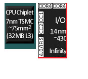
2x 7nm chiplets + half of the io 14nm die (its not getting moved to 7nm)
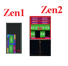
The 2 chiplets size is about 70-80% of current 2x zen1
Adding half the io
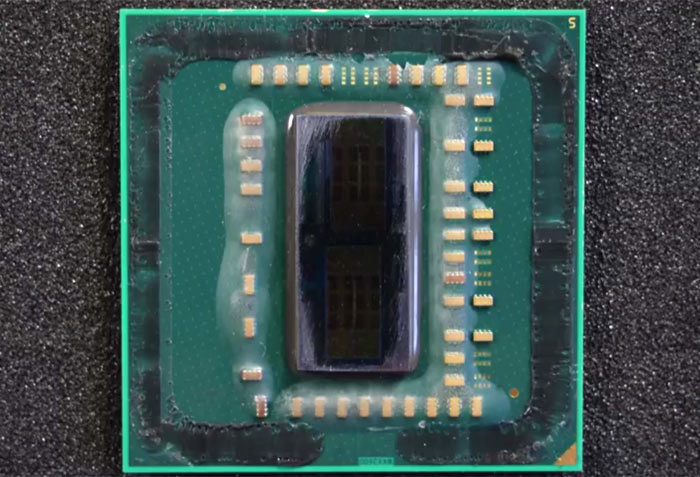
for one you are producing far bigger piece of silicon (total) on the chip, making it far more expensive than zen1. Not to mention socket sizing;
This is zen1 ryzen silicon;
if we were to make it with zen2 sizing (correct ratio)
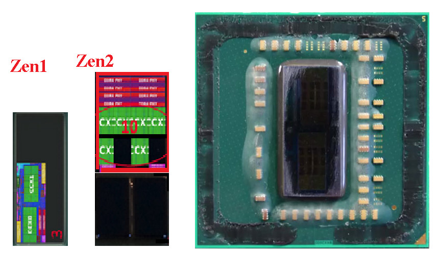
sure i’d be cheaper to produce the 2 7nm chiplets vs 2 14nm nodes… Tho the 14nm IO on its own will be taking around 60% of whole chip.
(and this is just to look fine; but the io die would have to be splited vertically not horizontally.)

and i believe that’s why the leak is false…
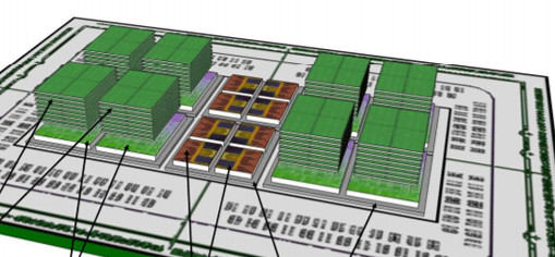
This is what i believe a look of correct zen2 ryzen die.
it should be to be supported on am4 x370|x470:
and it’ll likely be 2800/x; it would not only fit nicely on am4 socket, but would be cheaper to produce.
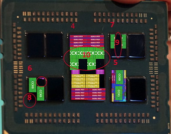
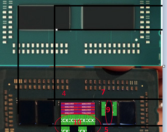
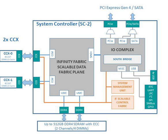
(each ~112mm^2 of io die also called sc-2, contains 2x CCX, (thus in fact you can use 1/4 size IO to connect 2 chiplets later in the game.)
and here you can see old concept render from amd
// IO seems to have changed, and have less scalability.
2 Likes
Locked and loaded 
That’s a good point, but I think the major benefit there is the surface area on the heat spreader. I’m not saying it’s impossible, just that I’m skeptical.
Ryzen uses 1/4 of an Epyc IO die, not 1/2… (2 chiplets not 8, 2x DDR4, not 8x DDR4, 1/4 of the PCIe or less, etc.).
The IO die is split BOTH horizontally AND vertically. So it’s 30% of the space, not 60% as per your maths…
Additionally, according to TSMC (or was it AMD?) their 7nm is half the physical space requirement of their 14nm.
Now, remember you took all the IO and memory controller (and maybe a lot of cache) out of the Ryzen 1 die. So the 7nm chiplets will be potentially <50% of the size of ryzen 1… the IO die will be 1/4 the size of Epycs.
6 Likes
I was going to speak to this, but you beat me to it. @anon5205053 brings up some valid concerns about space, but I don’t think the math is quite right on the post.
Theres also a lot of unused space on those am4 substrate.
You don’t need to keep those little surface mount components in the position they’re currently in. They can and will move, in ryzen 3rd Gen units.
4 Likes
My suspicion is that you’d have approximately 30% of the substrate left over (assuming 1x 1/4 epyc IO die and 2x chiplets), by rough visual gauge and assuming that the chiplets are exactly 50% of ryzen 1 die size. My bet is they’re significantly smaller than that though, unless they have a shit-tonne of on-die cache that hasn’t been pushed back to the IO controller.
And that may well be the case, to hide the latency incurred by moving the IO and memory controller off-die.
TLDR: there’s plenty of space on AM4 for what AdoredTV has claimed they’re doing, imho.
1 Like
I’m guessing closer to 42% for an 8 core chiplet, but we will see. Infinity fabric, ddr, pcie, etc take up a fair bit of space.
One thing that you guys need to keep in mind is that those cuts take up some space. This is especially the case with the IO chip if it is really build to be able to be split into 4 separate IO controllers. This on it’s own would be an impressive engineering feat and I hope this will be the case but everyone makes it sound like this is the obvious choice.
It would be amazing if true though. Also just think about the amount of bandwith that now needs to go through the organic substrate. This is some insanely impressive stuff.
2 Likes
Well, if so, they’ll include that on the design. I don’t think they’ll decide to chop it up as an afterthought.
Yeah, substrate heat production is actually starting to come into play.
Definitely.
I’d say that was the plan from the outset. I’d say all these decisions on modular design were made from the outset before Ryzen 1 even shipped.
Ryzen 1 would have been the alpha test variant of the new core without trying to be TOO tricky with the modularity. A clean sheet core design is already risky enough.
Ryzen 2’s changes are IMHO where we are seeing the true intent of AMDs design.
I see this also being linked to the decisions made in Vega to use HBCC and the same infinity fabric as Ryzen.
Being able to plug Vega (or Navi or whatever descendant carrying a future iteration of the HBCC/Infinity Fabric tech) into one of these IO dies along with some local HBM2/HBM3 for cache for main memory (connected direct to the IO controller die) is where Ryzen 3 will be going IMHO.
If you’re rocking a few gigs of HBM on package as cache for BOTH the CPU and GPU, you could even stretch DDR4 a lot further before DDR5 arrives.
6 Likes
These decisions, if true, were made probably around 2014-2015.
Amd really went all in on 7nm modular designs.
I think the 1 series was just a tech preview. There’s a reason so few companies adopted it, but are now looking to adopt 2nd Gen.
4gb of hbm2 on a 3990wx that acts as l4 cache or gpu mem, depending on what’s needed? Damn. 
Puts 1950x into hype jar
It’s all connected. Amd has truly been working towards something major.
The real question is, are we going to see a resurgence of multi-chip GPUs for gaming? I think infinity fabric can see some major improvements in microstutter and whatnot. It’s just a matter of game developer transparency.
4 Likes
That’s what i’m talking about.
Memory bandwidth has been lagging behind cores for decades. HBM on package for CPU is so frickin obvious IMHO. Sure, expensive. But the GPU will end up there eventually anyway, and if you’re putting the GPU there it needs a large amount of high bandwidth memory.
With HBCC you can push the bulk of the GPU’s memory out to main memory and still not tank too hard on performance. And if you have local HBM for the GPU, why not give the CPU a piece? Even more so with the high core counts on a single socket now.
In the past 20+ years I’ve spent in this game i’ve seen more and more stuff moved to the CPU/SOC. Floating Point. Audio. Modems, baseline VGA graphics. Now 3d graphics, and eventually top flight GPU cores.
2 Likes
Lets put it this way. The difference in price between say a Ryzen (or even Threadripper) 16 core and X299 16 core today is what?
That’s a lot of budget for local HBM if they wanted to. Just sayin’…
4 Likes
Dude, give me a apu that does 4k60 stable with 12/16gb and 8-12 cores at 4.x ghz on a single die? I’d pay 1200 for that easy.
So much has moved. We used to have northbridge and Southbridge, now it’s a single chipset that provides comms.
I can’t wait to see what comes next, but what about power output? Are we gonna see mandatory water cooling because an apu hits 450w from the factory?
2 Likes
Nah.
What was top of the line, 150-200 watt GPUs last decade is blown away by an IGP today.
The march to iGPU performance being “plenty” for end users will be slow, but it will be relentless.
I give discrete non-enterprise GPUs 3-4 remaining generations at best.
2 Likes