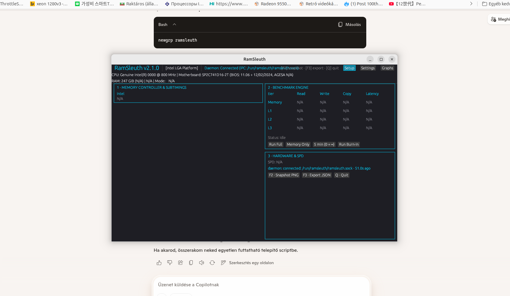
RamSleuth — RAM telemetry + memory benchmark for Linux

RamSleuth — live RAM telemetry + a real benchmark, for Linux

I built RamSleuth because I wanted to see what my RAM was actually doing right now while using linux, not a snapshot tool I have to go hunting for. It’s a live memory-telemetry suite and benchmark for Linux desktops, AMD and Intel, in pure Rust: it watches the memory controller’s real operating state and measures your memory subsystem.

What it does

Live memory telemetry. The daemon reads the memory controller’s own state and lays it out in one dashboard:

  • clocks — memory / controller / fabric, plus the command rate,
  • the live DRAM subtimings — the values the controller is running right now, not the ones baked into an XMP profile,
  • SPD for every DIMM — maker, DRAM die, density, rank, base speed, and the factory XMP / EXPO profiles,
  • channel mode, ECC status, and the voltage rails.

A real benchmark. A 4×4 grid — DRAM / L1 / L2 / L3 × Read / Write / Copy / Latency — with native AVX2 and AVX-512 kernels, one worker pinned per physical core (it falls back to AVX2 on CPUs without AVX-512). There’s an optional burn-in soak that re-runs the passes for hours if you want to stress-test stability.

Three frontends, same data. A desktop GUI, a 17-key terminal TUI, and a CLI. Pick your poison — it’s the same live readout under each.

Hardware coverage. AMD Ryzen and Intel desktop, Skylake through Arrow Lake, including DDR5. Where a part genuinely doesn’t expose the registers, I made the app say so plainly.

One-click setup. On first run, a single Set up RamSleuth click does all the privileged work: starts the daemon, grants your account socket access (no re-login), and builds + loads the kernel driver via DKMS — ryzen_smu on AMD, the ramsleuth_intel IMC module on Intel. Secure Boot is handled for you: a one-time MOK key enrollment + reboot, or just turn it off. It’s non-interactive and self-healing.

Under the hood. One small root daemon holding only CAP_SYS_RAWIO; every client you look at runs fully unprivileged. A missing driver, privilege, or piece of hardware never crashes anything — the affected fields just read a structured N/A (<reason>) and the process exits 0.

Getting it

Arch / AUR — pick exactly one of the two main packages:

  • ramsleuth-bin — prebuilt, install and go (fastest).
  • ramsleuth — builds from the official release tag (auditable source).
yay -S ramsleuth-bin   # or: yay -S ramsleuth

All bundle the driver sources, so the one-click setup works out of the box. If you just want the kernel driver on its own, the two optional standalone extras are ryzen-smu-dkms (AMD) and ramsleuth-intel-dkms (Intel).

Changelog

2.4.16

  • Intel readouts dual-channel kits resolve correctly and the memory-speed readout is accurate (no more doubled MT/s).
  • The benchmark is now the Memory & Latency Benchmark — it measures each tier (DRAM + L1/L2/L3) honestly, with a fast latency pass.
  • AMD coverage widened — Zen 4/5 and beyond now identify and decode fully instead of reading “unsupported.”
  • One source of truth across the TUI, GUI, and CLI — plus a cleaner graph, a readable probe report, and a live burn-in timer.
  • More to come

2.4.14

  • Intel CPU identification fixed across the modern lineup (the shared-model collision set), so more boxes resolve to the right generation and decode fully instead of reading “unsupported.”
  • Robust channel-mode detection, cross-checked against the firmware memory map — a populated dual-channel kit no longer misreads as single.
  • New board-delivered Intel vCore from the Super I/O chip, with an honest verified / [est] / N/A confidence badge.
  • The AUR source build now tunes to your CPU (native target-cpu with a safe 3-tier fallback).

Earlier highlights

  • 2.4.11 — the one-click setup is genuinely one click: daemon, access, and driver build all in a single privileged pass.
  • 2.4.9 — every N/A now explains itself in plain language; “no data on this part” is a healthy state, not an error.
  • 2.4.5 — SPD re-baselined to the JESD standard, and ECC detection on both AMD and Intel.
  • 2.4.2 — Intel expanded to Tier 3 (Alder / Raptor / Meteor / Arrow Lake, DDR5) + the consent-gated probe report.
  • 2.3.0 — Intel parity: live DRAM subtimings on Intel.
  • 2.2.0 — the one-click setup landed, and the AUR two-package release model was established.

A note on the odd ones

Feedback and bug reports are welcome — and if your machine reports something odd (or a clean N/A you don’t get), the one-click probe report packages up the system identity, the decoded readout, the raw register dump, and every N/A reason, so it’s easy to hand me the evidence.

Links

As always, feedback is more than welcome. Thanks!

4 Likes

1 Like

–EDIT– I have found the issue, thank you for bringing this up, I would not have found it had you not. I will be fixing it and releasing an update shortly. Thanks again.

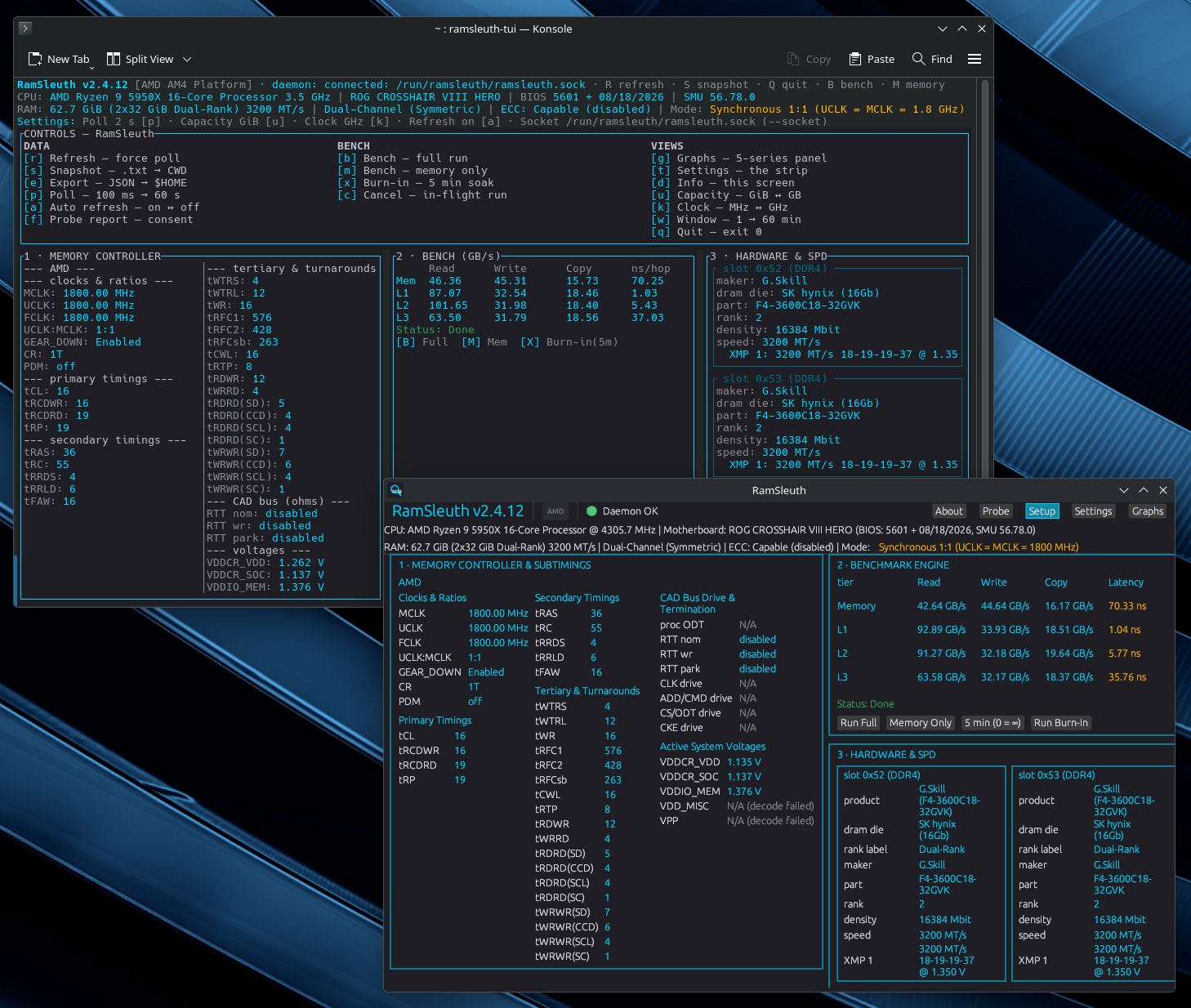
Bump — a lot has landed since I first shared this, and it’s at 2.4.12 now.

The change I’m most happy about: setup is finally a real one-click. Install from the AUR (yay -S ramsleuth-bin), open the app, and hit “Set up RamSleuth” — it takes care of the daemon, your access to it, and building/loading the kernel driver for you, Secure Boot included (with a clear one-time step if that’s on). The terminal fumbling is gone, and if it ever can’t do something it tells you exactly why.

A few other things that have come along since the original post:

  • Intel support now spans Skylake → Arrow Lake, including DDR5 — the extra subchannels and the memory-controller latency blocks, not just the basic timing set.
  • Channel mode (dual symmetric / flex, single, triple) and ECC status on both AMD and Intel.
  • SPD decoding re-baselined to the actual JESD specs — real manufacturer (JEP106), density, rank, base speed, and XMP 2.0 / 3.0 / EXPO profiles.
  • Self-explanatory readouts: every “N/A” now says why (“this part doesn’t expose those registers”, “that firmware version isn’t in the supported set”, “driver not loaded”), so you can tell “just no data on this part” from a real problem at a glance.
  • A one-click diagnostic “probe report” you can attach to a bug report, so nobody has to dig through logs.

The core design is the same as before: one small privileged daemon holding only CAP_SYS_RAWIO, with every client (GUI / TUI / CLI) running unprivileged.

Full details are in the OP above. As always, feedback and bug reports are very welcome — and if a machine reports something you don’t expect, the probe report makes it easy to show me.

1 Like

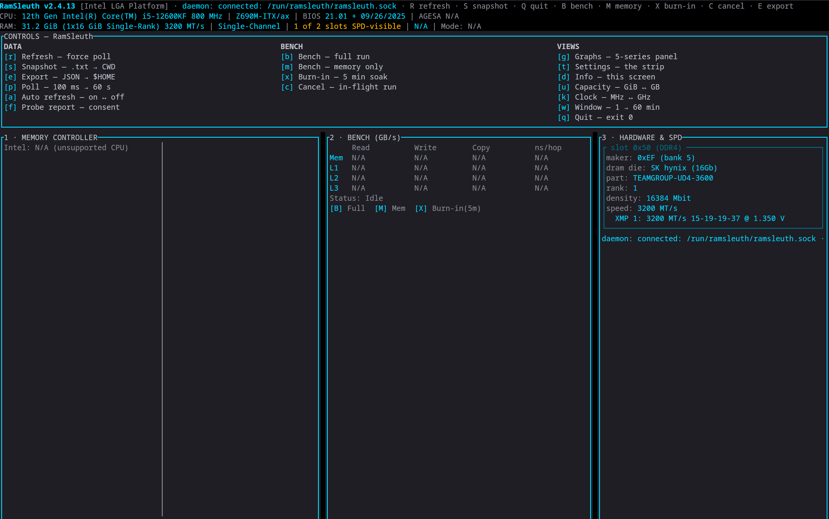
Replying here so as to not clutter the other thread, and as I have relevant feedback. Working with DeepSeek V4.1 Flash to get a Gentoo OpenRC version of install.sh working (done), running into another issue: The cpuid.rs table mis-matches the Intel CPUIDs. It’s flagging my 12600KF as TigerLake and then claiming it’s an unsupported CPU:

I assume the single-channel claim (it’s a 2x16GB kit, so dual channel) is due to it not reading the memory controller right.

These Intel chips also don’t seem to expose VDDC voltages on Linux (correct me if I’m wrong), they have the internal VID but that’s what the chip requests. The motherboard Super I/O is the reliable way to get the actual input vCore. On my system I’m seeing a ~0.04-0.6v delta between VID (requested voltage) and in0 on the NCT6798 Super I/O chip (the actual board delivered vCore), VID being the higher number. I run an undervolt and the middling load-line calibration setting, so it’s about what I’d expect.

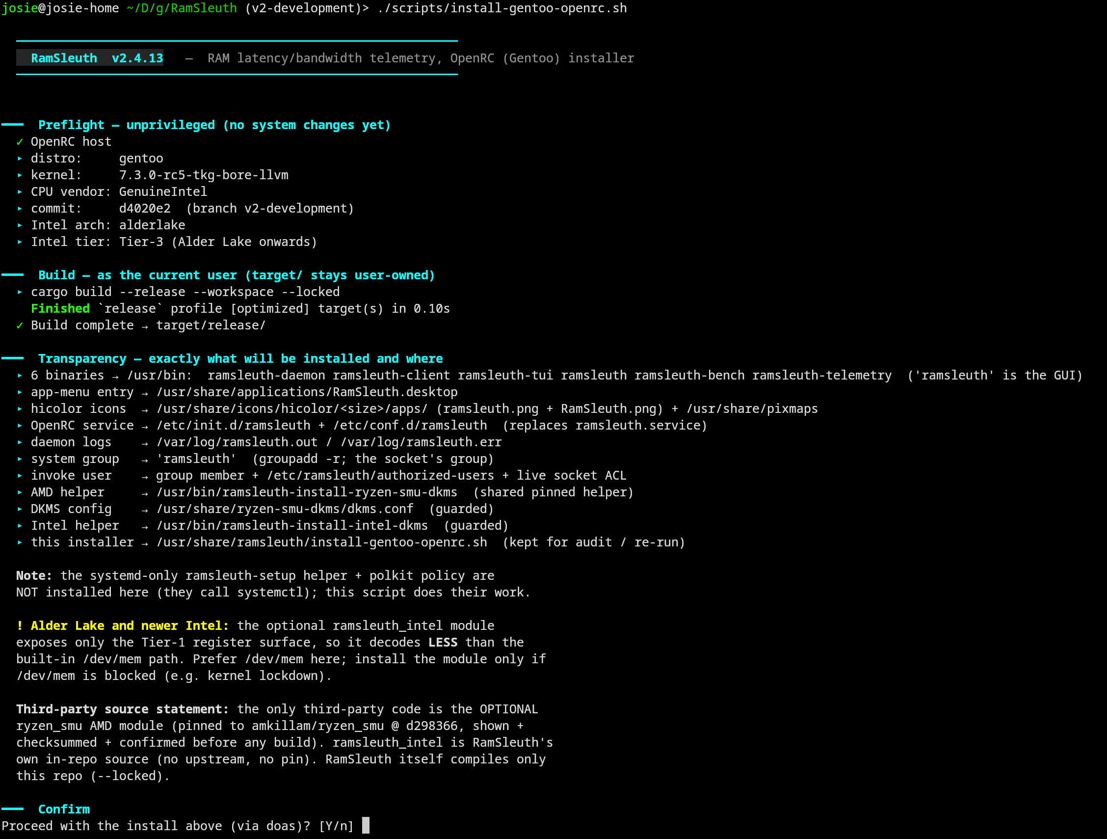
The install script was patched to use rustc’s target-cpus to read the arch, so it does pull it correctly, and adds the note that the kernel mod will actually display less information for this platform and newer:

Let me know if you want the gentoo script once I’m done (I don’t know if you want to offer it or not). I can make an issue on the repo and upload the text file, or do a fork → PR.

2 Likes

Hey thanks for the work and feedback!

I’m going to start looking into this today and spend some time fleshing out the intel side of things as much as I can without the hardware on hand. I’ve done some digging into and reading up on the new intel arch’s and have already found some things that need to be fixed done differently. Once I have a release out, I’ll post here and if you’re willing to lend a hand and give some feedback again, that’d be great!

Thanks again.

1 Like

Awesome! If you need any specific tests ran/numbers pulled, I can do so on my 12600KF machine. I have some older machines in the e-waste pile at work too, they’ve got Skylake chips in them, if you want pre-Alder numbers.

EDIT: Oh, if you want weird Intel too, I’ve got a Goldmont Plus (Gemini Lake) mini laptop as well. Little celeron-atom thingamabob.

1 Like

2.4.14 is out, it’s mostly an Intel love letter this round. The short version: modern Intel parts (12th/13th/14th gen through Core Ultra / Arrow / Lunar Lake) finally identify correctly (I’m hoping) so a lot more boxes should work, a populated dual-channel kit reads as dual-channel again (no more false “single-channel”), and Intel now shows real board-delivered core voltage (vCore if it can interface with sys chip) with an honest verified/estimate/N/A badge — matching what AMD already had. Both AUR packages (ramsleuth / ramsleuth-bin) are updated. The first post has the full breakdown.

@ZandoBob If you can / will test and give me feedback, I’d be grateful for any and all of it. THANKS!

1 Like

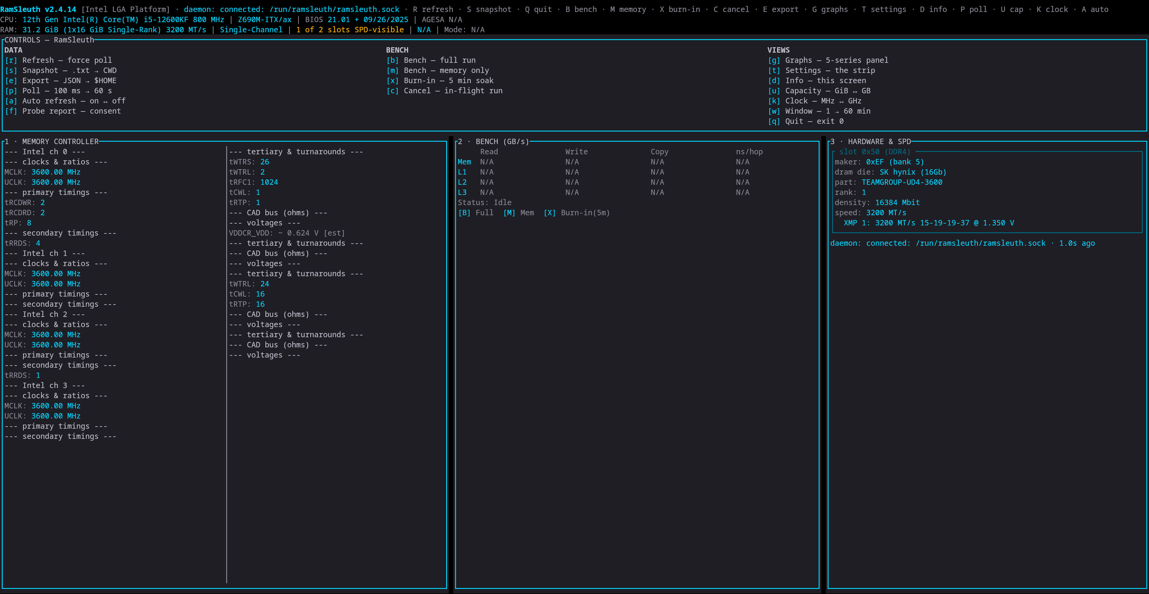
Checking it out now:

It’s now picking up the vcore reading!

Still thinks it’s single-channel though, digging into why now with DeepSeek. In the meantime, a couple UI notes:

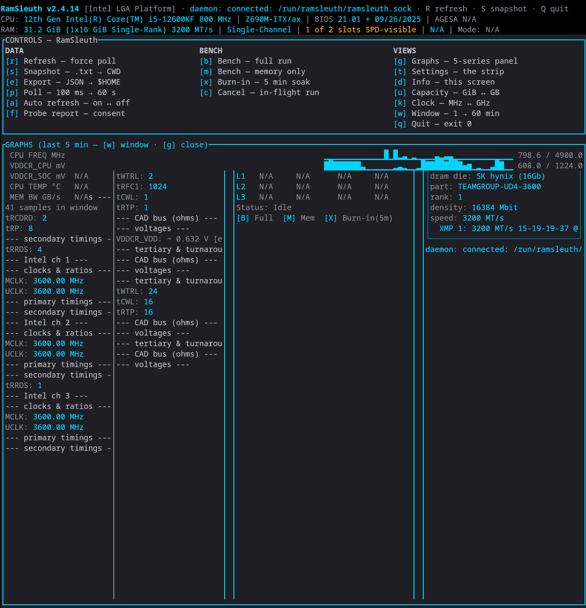
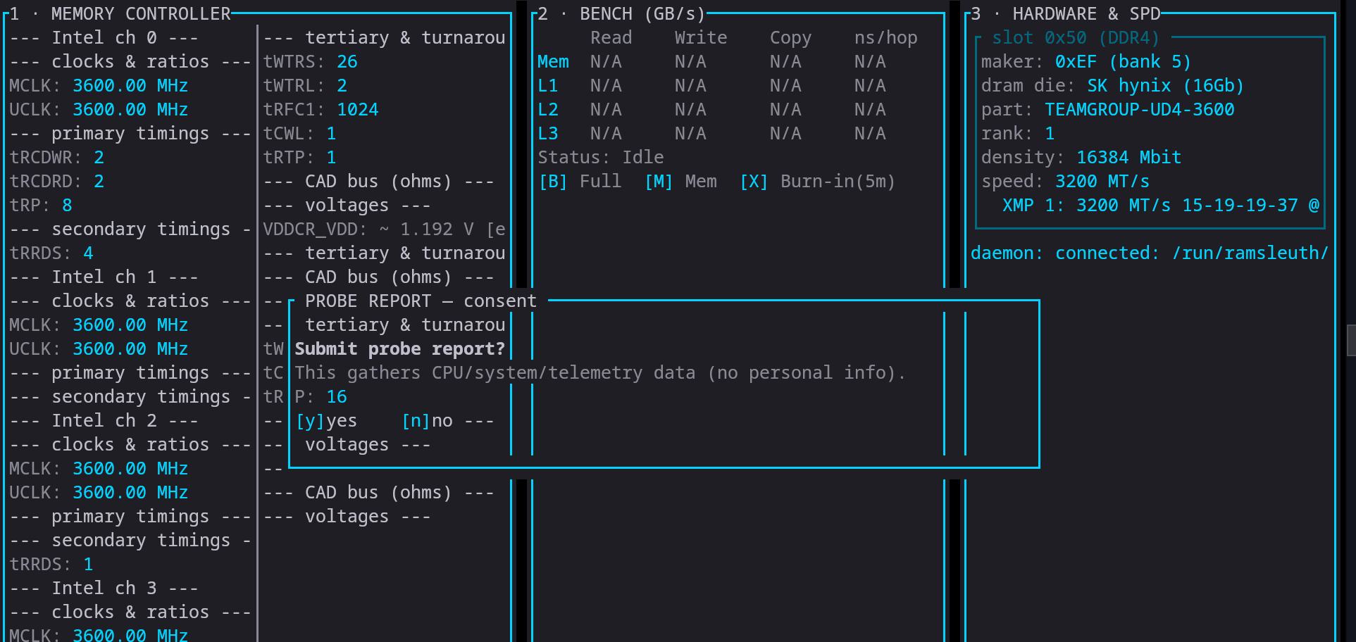
The graph function doesn’t re-draw the rest of the terminal window section below it, so those values just sit there, makes it hard to read. The probe report option also does this, only over-writing the blue border and the consent buttons, so it’s nigh impossible to read:

On the burn-in test, the “#:## elapsed” counter doesn’t tick up. I think that’s all the UI bugs I can find so far.

I can’t upload .md files, so here’s a paste of the probe report in a hide section, so it won’t make everyone scroll a million years :smiley:.

probe-report

RamSleuth Probe Report

12th Gen Intel(R) Core™ i5-12600KF — AlderLake on linux (kernel 7.3.0-rc5-tkg-bore-llvm), RamSleuth v2.4.14

System

Field Value
CPU 12th Gen Intel(R) Core™ i5-12600KF
Vendor Intel
Generation AlderLake
PCI Host Bridge 0x4648
Kernel 7.3.0-rc5-tkg-bore-llvm
OS linux
Arch x86_64
RamSleuth Version 2.4.14
Telemetry Source dev-mem

Decoded Telemetry

CPU

Field Value
vendor Intel AlderLake
brand 12th Gen Intel(R) Core™ i5-12600KF
CPU Core Voltage 0.704 V [est]

AMD

N/A (unsupported hardware)

Intel

Field Value
channel mode Single-Channel

Channel 0

Clock Value
MCLK 3600.00 MHz
MT/s 7200 MT/s
UCLK 3600.00 MHz
FCLK N/A (not applicable)
UCLK:MCLK N/A (not applicable)
gear mode 1x
GDM N/A (not applicable)
PDM N/A (not applicable)
command rate N/A (not applicable)
Timing (ticks) Value
tCL N/A (parse error: tCL 0 ticks outside plausible range [1, 2048])
tRCDWR 2
tRCDRD 2
tRP 8
tRAS N/A (parse error: tRAS 0 ticks outside plausible range [1, 2048])
tRC N/A (not applicable)
tRRDS 4
tRRLD N/A (parse error: tRRD_L 0 ticks outside plausible range [1, 2048])
tFAW N/A (parse error: tFAW 0 ticks outside plausible range [1, 2048])
tWTRS 26
tWTRL 2
tWR N/A (parse error: tWR 0 ticks outside plausible range [1, 2048])
tRFC1 1024
tRFC2 N/A (not applicable)
tRFCsb N/A (parse error: tRFCsb 0 ticks outside plausible range [1, 2048])
tCWL 1
tRTP 1
tRDWR N/A (not applicable)
tWRRD N/A (not applicable)
tRDRD(SD) N/A (parse error: tRDRD(dr) 0 ticks outside plausible range [1, 2048])
tRDRD(CCD) N/A (parse error: tRDRD(dd) 0 ticks outside plausible range [1, 2048])
tRDRD(SCL) N/A (parse error: tRDRD(sg) 0 ticks outside plausible range [1, 2048])
tRDRD(SC) N/A (parse error: tRDRD(dg) 0 ticks outside plausible range [1, 2048])
tWRWR(SD) N/A (not applicable)
tWRWR(CCD) N/A (not applicable)
tWRWR(SCL) N/A (parse error: tWRWR(sg) 0 ticks outside plausible range [1, 2048])
tWRWR(SC) N/A (parse error: tWRWR(dg) 0 ticks outside plausible range [1, 2048])
CAD bus (ohms) Value
proc ODT N/A (not applicable)
RTT nom N/A (not applicable)
RTT wr N/A (not applicable)
RTT park N/A (not applicable)
CLK drive N/A (not applicable)
ADD/CMD drive N/A (not applicable)
CS/ODT drive N/A (not applicable)
CKE drive N/A (not applicable)
Rail (V) Value
VDDCR_SOC N/A (not applicable)
VDDIO_MEM N/A (not applicable)
VDD_MISC N/A (not applicable)
VPP N/A (not applicable)
RTL (ticks) Value
RTL N/A (not applicable)

Channel 1

Clock Value
MCLK 3600.00 MHz
MT/s 7200 MT/s
UCLK 3600.00 MHz
FCLK N/A (not applicable)
UCLK:MCLK N/A (not applicable)
gear mode 1x
GDM N/A (not applicable)
PDM N/A (not applicable)
command rate N/A (not applicable)
Timing (ticks) Value
tCL N/A (parse error: tCL: register read failed)
tRCDWR N/A (parse error: tRCD: register read failed)
tRCDRD N/A (parse error: tRCD: register read failed)
tRP N/A (parse error: tRP: register read failed)
tRAS N/A (parse error: tRAS: register read failed)
tRC N/A (not applicable)
tRRDS N/A (parse error: tRRD_S: register read failed)
tRRLD N/A (parse error: tRRD_L: register read failed)
tFAW N/A (parse error: tFAW: register read failed)
tWTRS N/A (parse error: tWTR_S: register read failed)
tWTRL N/A (parse error: tWTR_L: register read failed)
tWR N/A (parse error: tWR: register read failed)
tRFC1 N/A (parse error: tRFC1: register read failed)
tRFC2 N/A (not applicable)
tRFCsb N/A (parse error: tRFCsb: register read failed)
tCWL N/A (parse error: tCWL: register read failed)
tRTP N/A (parse error: tRTP: register read failed)
tRDWR N/A (not applicable)
tWRRD N/A (not applicable)
tRDRD(SD) N/A (parse error: tRDRD(dr): register read failed)
tRDRD(CCD) N/A (parse error: tRDRD(dd): register read failed)
tRDRD(SCL) N/A (parse error: tRDRD(sg): register read failed)
tRDRD(SC) N/A (parse error: tRDRD(dg): register read failed)
tWRWR(SD) N/A (not applicable)
tWRWR(CCD) N/A (not applicable)
tWRWR(SCL) N/A (parse error: tWRWR(sg): register read failed)
tWRWR(SC) N/A (parse error: tWRWR(dg): register read failed)
CAD bus (ohms) Value
proc ODT N/A (not applicable)
RTT nom N/A (not applicable)
RTT wr N/A (not applicable)
RTT park N/A (not applicable)
CLK drive N/A (not applicable)
ADD/CMD drive N/A (not applicable)
CS/ODT drive N/A (not applicable)
CKE drive N/A (not applicable)
Rail (V) Value
VDDCR_SOC N/A (not applicable)
VDDIO_MEM N/A (not applicable)
VDD_MISC N/A (not applicable)
VPP N/A (not applicable)
RTL (ticks) Value
RTL N/A (not applicable)

Channel 2

Clock Value
MCLK 3600.00 MHz
MT/s 7200 MT/s
UCLK 3600.00 MHz
FCLK N/A (not applicable)
UCLK:MCLK N/A (not applicable)
gear mode 1x
GDM N/A (not applicable)
PDM N/A (not applicable)
command rate N/A (not applicable)
Timing (ticks) Value
tCL N/A (parse error: tCL 0 ticks outside plausible range [1, 2048])
tRCDWR N/A (parse error: tRCD 0 ticks outside plausible range [1, 2048])
tRCDRD N/A (parse error: tRCD 0 ticks outside plausible range [1, 2048])
tRP N/A (parse error: tRP 0 ticks outside plausible range [1, 2048])
tRAS N/A (parse error: tRAS 0 ticks outside plausible range [1, 2048])
tRC N/A (not applicable)
tRRDS 1
tRRLD N/A (parse error: tRRD_L 0 ticks outside plausible range [1, 2048])
tFAW N/A (parse error: tFAW 0 ticks outside plausible range [1, 2048])
tWTRS N/A (parse error: tWTR_S 0 ticks outside plausible range [1, 2048])
tWTRL 24
tWR N/A (parse error: tWR 0 ticks outside plausible range [1, 2048])
tRFC1 N/A (parse error: tRFC1 0 ticks outside plausible range [1, 2048])
tRFC2 N/A (not applicable)
tRFCsb N/A (parse error: tRFCsb 0 ticks outside plausible range [1, 2048])
tCWL 16
tRTP 16
tRDWR N/A (not applicable)
tWRRD N/A (not applicable)
tRDRD(SD) N/A (parse error: tRDRD(dr) 0 ticks outside plausible range [1, 2048])
tRDRD(CCD) N/A (parse error: tRDRD(dd) 0 ticks outside plausible range [1, 2048])
tRDRD(SCL) N/A (parse error: tRDRD(sg) 0 ticks outside plausible range [1, 2048])
tRDRD(SC) N/A (parse error: tRDRD(dg) 0 ticks outside plausible range [1, 2048])
tWRWR(SD) N/A (not applicable)
tWRWR(CCD) N/A (not applicable)
tWRWR(SCL) N/A (parse error: tWRWR(sg) 0 ticks outside plausible range [1, 2048])
tWRWR(SC) N/A (parse error: tWRWR(dg) 0 ticks outside plausible range [1, 2048])
CAD bus (ohms) Value
proc ODT N/A (not applicable)
RTT nom N/A (not applicable)
RTT wr N/A (not applicable)
RTT park N/A (not applicable)
CLK drive N/A (not applicable)
ADD/CMD drive N/A (not applicable)
CS/ODT drive N/A (not applicable)
CKE drive N/A (not applicable)
Rail (V) Value
VDDCR_SOC N/A (not applicable)
VDDIO_MEM N/A (not applicable)
VDD_MISC N/A (not applicable)
VPP N/A (not applicable)
RTL (ticks) Value
RTL N/A (not applicable)

Channel 3

Clock Value
MCLK 3600.00 MHz
MT/s 7200 MT/s
UCLK 3600.00 MHz
FCLK N/A (not applicable)
UCLK:MCLK N/A (not applicable)
gear mode 1x
GDM N/A (not applicable)
PDM N/A (not applicable)
command rate N/A (not applicable)
Timing (ticks) Value
tCL N/A (parse error: tCL: register read failed)
tRCDWR N/A (parse error: tRCD: register read failed)
tRCDRD N/A (parse error: tRCD: register read failed)
tRP N/A (parse error: tRP: register read failed)
tRAS N/A (parse error: tRAS: register read failed)
tRC N/A (not applicable)
tRRDS N/A (parse error: tRRD_S: register read failed)
tRRLD N/A (parse error: tRRD_L: register read failed)
tFAW N/A (parse error: tFAW: register read failed)
tWTRS N/A (parse error: tWTR_S: register read failed)
tWTRL N/A (parse error: tWTR_L: register read failed)
tWR N/A (parse error: tWR: register read failed)
tRFC1 N/A (parse error: tRFC1: register read failed)
tRFC2 N/A (not applicable)
tRFCsb N/A (parse error: tRFCsb: register read failed)
tCWL N/A (parse error: tCWL: register read failed)
tRTP N/A (parse error: tRTP: register read failed)
tRDWR N/A (not applicable)
tWRRD N/A (not applicable)
tRDRD(SD) N/A (parse error: tRDRD(dr): register read failed)
tRDRD(CCD) N/A (parse error: tRDRD(dd): register read failed)
tRDRD(SCL) N/A (parse error: tRDRD(sg): register read failed)
tRDRD(SC) N/A (parse error: tRDRD(dg): register read failed)
tWRWR(SD) N/A (not applicable)
tWRWR(CCD) N/A (not applicable)
tWRWR(SCL) N/A (parse error: tWRWR(sg): register read failed)
tWRWR(SC) N/A (parse error: tWRWR(dg): register read failed)
CAD bus (ohms) Value
proc ODT N/A (not applicable)
RTT nom N/A (not applicable)
RTT wr N/A (not applicable)
RTT park N/A (not applicable)
CLK drive N/A (not applicable)
ADD/CMD drive N/A (not applicable)
CS/ODT drive N/A (not applicable)
CKE drive N/A (not applicable)
Rail (V) Value
VDDCR_SOC N/A (not applicable)
VDDIO_MEM N/A (not applicable)
VDD_MISC N/A (not applicable)
VPP N/A (not applicable)
RTL (ticks) Value
RTL N/A (not applicable)

SPD

Module 0x50 (DDR4)

Field Value
maker 0xEF (bank 5)
die maker SK hynix
die type N/A (not applicable)
devices 8
part TEAMGROUP-UD4-3600
serial 0104D817
rank 1
density 16384 Mbit
speed 3200 MT/s
  • profile 1 (XMP): 3200 MT/s, 15-19-19-37 @ 1.350 V

Platform

Field Value
CPU clock (MHz) 799.15 MHz
motherboard Z690M-ITX/ax
BIOS 21.01 + 09/26/2025
AGESA N/A (not applicable)
SMU version N/A (not applicable)
total capacity 31.2 GiB
per-DIMM sizes 16.0 GiB

Raw Registers

Register Value
MC_BIOS_REQ 0x79E00124
TC_CH0_DBP 0xFFFFFFFF
TC_CH0_RAP 0xFFFFFFFF
TC_CH0_RFP 0xFFFFFFFF
TC_CH0_RAP2 0xFFFFFFFF
TC_CH0_RDRD 0xFFFFFFFF
TC_CH0_RDWR 0xFFFFFFFF
TC_CH0_WRRD 0xFFFFFFFF
TC_CH0_WRWR 0xFFFFFFFF
TC_CH1_DBP 0xFFFFFFFF
TC_CH1_RAP 0xFFFFFFFF
TC_CH1_RFP 0xFFFFFFFF
TC_CH1_RAP2 0xFFFFFFFF
TC_CH1_RDRD 0xFFFFFFFF
TC_CH1_RDWR 0xFFFFFFFF
TC_CH1_WRRD 0xFFFFFFFF
TC_CH1_WRWR 0xFFFFFFFF
TC_CH2_DBP 0xFFFFFFFF
TC_CH2_RAP 0xFFFFFFFF
TC_CH2_RFP 0xFFFFFFFF
TC_CH2_RAP2 0xFFFFFFFF
TC_CH2_RDRD 0xFFFFFFFF
TC_CH2_RDWR 0xFFFFFFFF
TC_CH2_WRRD 0xFFFFFFFF
TC_CH2_WRWR 0xFFFFFFFF
TC_CH3_DBP 0xFFFFFFFF
TC_CH3_RAP 0xFFFFFFFF
TC_CH3_RFP 0xFFFFFFFF
TC_CH3_RAP2 0xFFFFFFFF
TC_CH3_RDRD 0xFFFFFFFF
TC_CH3_RDWR 0xFFFFFFFF
TC_CH3_WRRD 0xFFFFFFFF
TC_CH3_WRWR 0xFFFFFFFF
MCL0_PRE 0x01000208
MCL0_ACT 0x00000400
MCL0_ACT2 0xFFFFFFFF
MCL0_WTR 0x0100021A
MCL0_RFP 0x00000400
MCL0_RFP2 0x00000000
MCL0_RDRD 0x00000000
MCL0_WRWR 0x00620000
MCL1_PRE 0x10000000
MCL1_ACT 0x00000100
MCL1_ACT2 0x00000000
MCL1_WTR 0x10001800
MCL1_RFP 0x00000000
MCL1_RFP2 0x00000000
MCL1_RDRD 0x00000000
MCL1_WRWR 0x00000000
MAD_INTER_CHANNEL N/A (absent)
MAD_INTRA_CH0 N/A (absent)
MAD_INTRA_CH1 N/A (absent)
MAD_DIMM_CH0 N/A (absent)
MAD_DIMM_CH1 N/A (absent)
MAD_DIMM_CH2 N/A (absent)
MAD_DIMM_CH3 N/A (absent)
MCHBAR_BASE 0xFEDC0000
MCHBAR_ENABLED true

N/A Reasons

  • amd (whole branch) — N/A (unsupported hardware)
  • intel.ch0.clocks.fclk — N/A (not applicable)
  • intel.ch0.clocks.div_mode — N/A (not applicable)
  • intel.ch0.clocks.gdm — N/A (not applicable)
  • intel.ch0.clocks.pdm — N/A (not applicable)
  • intel.ch0.clocks.command_rate — N/A (not applicable)
  • intel.ch0.timings.cl — N/A (parse error: tCL 0 ticks outside plausible range [1, 2048])
  • intel.ch0.timings.ras — N/A (parse error: tRAS 0 ticks outside plausible range [1, 2048])
  • intel.ch0.timings.rc — N/A (not applicable)
  • intel.ch0.timings.rrld — N/A (parse error: tRRD_L 0 ticks outside plausible range [1, 2048])
  • intel.ch0.timings.faw — N/A (parse error: tFAW 0 ticks outside plausible range [1, 2048])
  • intel.ch0.timings.wr — N/A (parse error: tWR 0 ticks outside plausible range [1, 2048])
  • intel.ch0.timings.rfc2 — N/A (not applicable)
  • intel.ch0.timings.rfcsb — N/A (parse error: tRFCsb 0 ticks outside plausible range [1, 2048])
  • intel.ch0.timings.rdwr — N/A (not applicable)
  • intel.ch0.timings.wrrd — N/A (not applicable)
  • intel.ch0.timings.rdrd_sd — N/A (parse error: tRDRD(dr) 0 ticks outside plausible range [1, 2048])
  • intel.ch0.timings.rdrd_dd — N/A (parse error: tRDRD(dd) 0 ticks outside plausible range [1, 2048])
  • intel.ch0.timings.rdrd_scl — N/A (parse error: tRDRD(sg) 0 ticks outside plausible range [1, 2048])
  • intel.ch0.timings.rdrd_sc — N/A (parse error: tRDRD(dg) 0 ticks outside plausible range [1, 2048])
  • intel.ch0.timings.wrwr_sd — N/A (not applicable)
  • intel.ch0.timings.wrwr_dd — N/A (not applicable)
  • intel.ch0.timings.wrwr_scl — N/A (parse error: tWRWR(sg) 0 ticks outside plausible range [1, 2048])
  • intel.ch0.timings.wrwr_sc — N/A (parse error: tWRWR(dg) 0 ticks outside plausible range [1, 2048])
  • intel.ch0.cad_bus.proc_odt — N/A (not applicable)
  • intel.ch0.cad_bus.rtt_nom — N/A (not applicable)
  • intel.ch0.cad_bus.rtt_wr — N/A (not applicable)
  • intel.ch0.cad_bus.rtt_park — N/A (not applicable)
  • intel.ch0.cad_bus.clk_drv — N/A (not applicable)
  • intel.ch0.cad_bus.addr_cmd_drv — N/A (not applicable)
  • intel.ch0.cad_bus.cs_odt_drv — N/A (not applicable)
  • intel.ch0.cad_bus.cke_drv — N/A (not applicable)
  • intel.ch0.voltages.vddcr_soc — N/A (not applicable)
  • intel.ch0.voltages.vddio_mem — N/A (not applicable)
  • intel.ch0.voltages.vdd_misc — N/A (not applicable)
  • intel.ch0.voltages.vpp — N/A (not applicable)
  • intel.ch0.rtl — N/A (not applicable)
  • intel.ch1.clocks.fclk — N/A (not applicable)
  • intel.ch1.clocks.div_mode — N/A (not applicable)
  • intel.ch1.clocks.gdm — N/A (not applicable)
  • intel.ch1.clocks.pdm — N/A (not applicable)
  • intel.ch1.clocks.command_rate — N/A (not applicable)
  • intel.ch1.timings.cl — N/A (parse error: tCL: register read failed)
  • intel.ch1.timings.rcwdwr — N/A (parse error: tRCD: register read failed)
  • intel.ch1.timings.rcdrd — N/A (parse error: tRCD: register read failed)
  • intel.ch1.timings.rp — N/A (parse error: tRP: register read failed)
  • intel.ch1.timings.ras — N/A (parse error: tRAS: register read failed)
  • intel.ch1.timings.rc — N/A (not applicable)
  • intel.ch1.timings.rrds — N/A (parse error: tRRD_S: register read failed)
  • intel.ch1.timings.rrld — N/A (parse error: tRRD_L: register read failed)
  • intel.ch1.timings.faw — N/A (parse error: tFAW: register read failed)
  • intel.ch1.timings.wtrs — N/A (parse error: tWTR_S: register read failed)
  • intel.ch1.timings.wtrl — N/A (parse error: tWTR_L: register read failed)
  • intel.ch1.timings.wr — N/A (parse error: tWR: register read failed)
  • intel.ch1.timings.rfc1 — N/A (parse error: tRFC1: register read failed)
  • intel.ch1.timings.rfc2 — N/A (not applicable)
  • intel.ch1.timings.rfcsb — N/A (parse error: tRFCsb: register read failed)
  • intel.ch1.timings.cwl — N/A (parse error: tCWL: register read failed)
  • intel.ch1.timings.rtp — N/A (parse error: tRTP: register read failed)
  • intel.ch1.timings.rdwr — N/A (not applicable)
  • intel.ch1.timings.wrrd — N/A (not applicable)
  • intel.ch1.timings.rdrd_sd — N/A (parse error: tRDRD(dr): register read failed)
  • intel.ch1.timings.rdrd_dd — N/A (parse error: tRDRD(dd): register read failed)
  • intel.ch1.timings.rdrd_scl — N/A (parse error: tRDRD(sg): register read failed)
  • intel.ch1.timings.rdrd_sc — N/A (parse error: tRDRD(dg): register read failed)
  • intel.ch1.timings.wrwr_sd — N/A (not applicable)
  • intel.ch1.timings.wrwr_dd — N/A (not applicable)
  • intel.ch1.timings.wrwr_scl — N/A (parse error: tWRWR(sg): register read failed)
  • intel.ch1.timings.wrwr_sc — N/A (parse error: tWRWR(dg): register read failed)
  • intel.ch1.cad_bus.proc_odt — N/A (not applicable)
  • intel.ch1.cad_bus.rtt_nom — N/A (not applicable)
  • intel.ch1.cad_bus.rtt_wr — N/A (not applicable)
  • intel.ch1.cad_bus.rtt_park — N/A (not applicable)
  • intel.ch1.cad_bus.clk_drv — N/A (not applicable)
  • intel.ch1.cad_bus.addr_cmd_drv — N/A (not applicable)
  • intel.ch1.cad_bus.cs_odt_drv — N/A (not applicable)
  • intel.ch1.cad_bus.cke_drv — N/A (not applicable)
  • intel.ch1.voltages.vddcr_soc — N/A (not applicable)
  • intel.ch1.voltages.vddio_mem — N/A (not applicable)
  • intel.ch1.voltages.vdd_misc — N/A (not applicable)
  • intel.ch1.voltages.vpp — N/A (not applicable)
  • intel.ch1.rtl — N/A (not applicable)
  • intel.ch2.clocks.fclk — N/A (not applicable)
  • intel.ch2.clocks.div_mode — N/A (not applicable)
  • intel.ch2.clocks.gdm — N/A (not applicable)
  • intel.ch2.clocks.pdm — N/A (not applicable)
  • intel.ch2.clocks.command_rate — N/A (not applicable)
  • intel.ch2.timings.cl — N/A (parse error: tCL 0 ticks outside plausible range [1, 2048])
  • intel.ch2.timings.rcwdwr — N/A (parse error: tRCD 0 ticks outside plausible range [1, 2048])
  • intel.ch2.timings.rcdrd — N/A (parse error: tRCD 0 ticks outside plausible range [1, 2048])
  • intel.ch2.timings.rp — N/A (parse error: tRP 0 ticks outside plausible range [1, 2048])
  • intel.ch2.timings.ras — N/A (parse error: tRAS 0 ticks outside plausible range [1, 2048])
  • intel.ch2.timings.rc — N/A (not applicable)
  • intel.ch2.timings.rrld — N/A (parse error: tRRD_L 0 ticks outside plausible range [1, 2048])
  • intel.ch2.timings.faw — N/A (parse error: tFAW 0 ticks outside plausible range [1, 2048])
  • intel.ch2.timings.wtrs — N/A (parse error: tWTR_S 0 ticks outside plausible range [1, 2048])
  • intel.ch2.timings.wr — N/A (parse error: tWR 0 ticks outside plausible range [1, 2048])
  • intel.ch2.timings.rfc1 — N/A (parse error: tRFC1 0 ticks outside plausible range [1, 2048])
  • intel.ch2.timings.rfc2 — N/A (not applicable)
  • intel.ch2.timings.rfcsb — N/A (parse error: tRFCsb 0 ticks outside plausible range [1, 2048])
  • intel.ch2.timings.rdwr — N/A (not applicable)
  • intel.ch2.timings.wrrd — N/A (not applicable)
  • intel.ch2.timings.rdrd_sd — N/A (parse error: tRDRD(dr) 0 ticks outside plausible range [1, 2048])
  • intel.ch2.timings.rdrd_dd — N/A (parse error: tRDRD(dd) 0 ticks outside plausible range [1, 2048])
  • intel.ch2.timings.rdrd_scl — N/A (parse error: tRDRD(sg) 0 ticks outside plausible range [1, 2048])
  • intel.ch2.timings.rdrd_sc — N/A (parse error: tRDRD(dg) 0 ticks outside plausible range [1, 2048])
  • intel.ch2.timings.wrwr_sd — N/A (not applicable)
  • intel.ch2.timings.wrwr_dd — N/A (not applicable)
  • intel.ch2.timings.wrwr_scl — N/A (parse error: tWRWR(sg) 0 ticks outside plausible range [1, 2048])
  • intel.ch2.timings.wrwr_sc — N/A (parse error: tWRWR(dg) 0 ticks outside plausible range [1, 2048])
  • intel.ch2.cad_bus.proc_odt — N/A (not applicable)
  • intel.ch2.cad_bus.rtt_nom — N/A (not applicable)
  • intel.ch2.cad_bus.rtt_wr — N/A (not applicable)
  • intel.ch2.cad_bus.rtt_park — N/A (not applicable)
  • intel.ch2.cad_bus.clk_drv — N/A (not applicable)
  • intel.ch2.cad_bus.addr_cmd_drv — N/A (not applicable)
  • intel.ch2.cad_bus.cs_odt_drv — N/A (not applicable)
  • intel.ch2.cad_bus.cke_drv — N/A (not applicable)
  • intel.ch2.voltages.vddcr_soc — N/A (not applicable)
  • intel.ch2.voltages.vddio_mem — N/A (not applicable)
  • intel.ch2.voltages.vdd_misc — N/A (not applicable)
  • intel.ch2.voltages.vpp — N/A (not applicable)
  • intel.ch2.rtl — N/A (not applicable)
  • intel.ch3.clocks.fclk — N/A (not applicable)
  • intel.ch3.clocks.div_mode — N/A (not applicable)
  • intel.ch3.clocks.gdm — N/A (not applicable)
  • intel.ch3.clocks.pdm — N/A (not applicable)
  • intel.ch3.clocks.command_rate — N/A (not applicable)
  • intel.ch3.timings.cl — N/A (parse error: tCL: register read failed)
  • intel.ch3.timings.rcwdwr — N/A (parse error: tRCD: register read failed)
  • intel.ch3.timings.rcdrd — N/A (parse error: tRCD: register read failed)
  • intel.ch3.timings.rp — N/A (parse error: tRP: register read failed)
  • intel.ch3.timings.ras — N/A (parse error: tRAS: register read failed)
  • intel.ch3.timings.rc — N/A (not applicable)
  • intel.ch3.timings.rrds — N/A (parse error: tRRD_S: register read failed)
  • intel.ch3.timings.rrld — N/A (parse error: tRRD_L: register read failed)
  • intel.ch3.timings.faw — N/A (parse error: tFAW: register read failed)
  • intel.ch3.timings.wtrs — N/A (parse error: tWTR_S: register read failed)
  • intel.ch3.timings.wtrl — N/A (parse error: tWTR_L: register read failed)
  • intel.ch3.timings.wr — N/A (parse error: tWR: register read failed)
  • intel.ch3.timings.rfc1 — N/A (parse error: tRFC1: register read failed)
  • intel.ch3.timings.rfc2 — N/A (not applicable)
  • intel.ch3.timings.rfcsb — N/A (parse error: tRFCsb: register read failed)
  • intel.ch3.timings.cwl — N/A (parse error: tCWL: register read failed)
  • intel.ch3.timings.rtp — N/A (parse error: tRTP: register read failed)
  • intel.ch3.timings.rdwr — N/A (not applicable)
  • intel.ch3.timings.wrrd — N/A (not applicable)
  • intel.ch3.timings.rdrd_sd — N/A (parse error: tRDRD(dr): register read failed)
  • intel.ch3.timings.rdrd_dd — N/A (parse error: tRDRD(dd): register read failed)
  • intel.ch3.timings.rdrd_scl — N/A (parse error: tRDRD(sg): register read failed)
  • intel.ch3.timings.rdrd_sc — N/A (parse error: tRDRD(dg): register read failed)
  • intel.ch3.timings.wrwr_sd — N/A (not applicable)
  • intel.ch3.timings.wrwr_dd — N/A (not applicable)
  • intel.ch3.timings.wrwr_scl — N/A (parse error: tWRWR(sg): register read failed)
  • intel.ch3.timings.wrwr_sc — N/A (parse error: tWRWR(dg): register read failed)
  • intel.ch3.cad_bus.proc_odt — N/A (not applicable)
  • intel.ch3.cad_bus.rtt_nom — N/A (not applicable)
  • intel.ch3.cad_bus.rtt_wr — N/A (not applicable)
  • intel.ch3.cad_bus.rtt_park — N/A (not applicable)
  • intel.ch3.cad_bus.clk_drv — N/A (not applicable)
  • intel.ch3.cad_bus.addr_cmd_drv — N/A (not applicable)
  • intel.ch3.cad_bus.cs_odt_drv — N/A (not applicable)
  • intel.ch3.cad_bus.cke_drv — N/A (not applicable)
  • intel.ch3.voltages.vddcr_soc — N/A (not applicable)
  • intel.ch3.voltages.vddio_mem — N/A (not applicable)
  • intel.ch3.voltages.vdd_misc — N/A (not applicable)
  • intel.ch3.voltages.vpp — N/A (not applicable)
  • intel.ch3.rtl — N/A (not applicable)
  • spd[0x50].die_type — N/A (not applicable)
  • platform.agesa — N/A (not applicable)
  • platform.smu_version — N/A (not applicable)
  • raw.mad_inter_channel — N/A (register absent / read failed)
  • raw.mad_intra_ch0 — N/A (register absent / read failed)
  • raw.mad_intra_ch1 — N/A (register absent / read failed)
  • raw.mad_dimm_ch0 — N/A (register absent / read failed)
  • raw.mad_dimm_ch1 — N/A (register absent / read failed)
  • raw.mad_dimm_ch2 — N/A (register absent / read failed)
  • raw.mad_dimm_ch3 — N/A (register absent / read failed)

This report was auto-generated by RamSleuth v2.4.14. It contains no personal information (no username, hostname, IP, MAC, or serial numbers).

Alright, DS figured it out. The collector looks at the dmi entry folder as a file, errors, the continue on error arg swallows it, so it reports 0. That way it never triggers the override guard. The test creates the mock entry as a file, so it passes. The parser is reading the wrong values on this system too. Here’s DS’s summary:

DeepSeek V4.1 Flash’s Report

The bug: intel_smbios::collect_from walks /sys/firmware/dmi/entries/, then reads each 17-<n> (17-0, 17-1 here) as if it were a file. On Linux sysfs each entry is a directory — the data is in 17-<n>/raw. std::fs::read on a directory errors, the loop’s Err(_) => continue swallows it, so every entry is skipped and populated_count stays 0. That means your L3 override guard (populated_count >= 2 && derived_mode == Dual) can never fire, so the MMIO Single is accepted as L1 VerifiedHardware.

Why the tests miss it: the fixture (write_entry in the test module) creates 17-<n> as a plain file, not a 17-<n>/raw directory, so fs::read succeeds there. The tests validate a layout the kernel never produces.

Fix #1 (the blocker): read path.join("raw").

Then the parser needs fixing too — the field offsets/indexing are off for this board (12600KF / Z690M-ITX/ax, DDR4):

  • Size is at 0x0C (word; bit 15 = MB/KB) with the 0x1C extended-size fallback — not 0x28, which here is Memory Technology (0x0000_0803, misread as 2051 MiB).
  • Locator string refs are at 0x10 (Device Locator) / 0x11 (Bank Locator) — not 0x06/0x0C (those are the Memory Error Handle and the Size word).
  • String-table indexing is off by one. string_at assumes the string area starts with an empty segment (parts[ref]), but a real SMBIOS table starts at the first string, so ref 1 is parts[0], not parts[1]. The fixture hides this too — type17_file does out.push(0) before the strings, injecting the empty segment the parser assumes. Fix: parts[ref - 1].
  • Channel classifier: this firmware names the DIMMs Controller0-ChannelA-DIMM0 and Controller1-ChannelA-DIMM0 — both say ChannelA; the channel is the Controller index. channel_of only matches standalone A–D tokens, so it can’t tell them apart → Ambiguous, never Dual.

With #1 + the parser fixes, this box reports populated_count: 2, dimm_sizes: [16384, 16384], locators Controller0-ChannelA-DIMM0/Controller1-ChannelA-DIMM0, derived_mode: Dual, and the live probe flips to DualSymmetric / Override / dimm_count: 2.

One aside: the override now correctly reports Dual, but the underlying MMIO decode still says Single on this host — so the register read at the 0xd800 base may be worth a look separately for DDR4 Alder Lake.


Optional extra: the full crate test run also fails a pre-existing test — intel_readout::tests::read_regs_on_this_host_is_structural_and_panic_free asserts ch.index == i, but this Alder Lake DDR4 host exposes subchannels 0,2, not 0,1. Separate from the channel-mode issue, but it’s a real failure on this hardware.

The patched version reads correctly:
channel_mode: Some(DualSymmetric)
channel_trust: Some(Override)
channel_annotation: "[Override: MCHBAR decoded Single-Channel
dimm_count: 2 }"

And here’s the raw hex dumps and dmidecode:

17-0/raw hex dump

0000000 11 5c 0c 00 0b 00 fe ff 40 00 40 00 00 40 09 00
0000016 01 02 1a 80 00 60 09 03 04 05 06 01 00 00 00 00
0000032 10 0e b0 04 46 05 b0 04 03 08 00 00 04 ef 00 00
0000048 00 00 00 00 00 00 00 00 00 00 00 00 00 00 00 00
0000064 04 00 00 00 00 00 00 00 00 00 00 00 00 00 00 00
0000080 00 00 00 00 00 00 00 00 00 00 00 00 43 6f 6e 74
0000096 72 6f 6c 6c 65 72 30 2d 43 68 61 6e 6e 65 6c 41
0000112 2d 44 49 4d 4d 30 00 42 41 4e 4b 20 30 00 54 65
0000128 61 6d 20 47 72 6f 75 70 20 49 6e 63 00 30 31 30
0000144 34 44 38 31 37 00 39 38 37 36 35 34 33 32 31 30
0000160 00 54 45 41 4d 47 52 4f 55 50 2d 55 44 34 2d 33
0000176 36 30 30 20 20 00 00
0000183

17-1/raw hex dump

0000000 11 5c 0d 00 0b 00 fe ff 40 00 40 00 00 40 09 00
0000016 01 02 1a 80 00 60 09 03 04 05 06 01 00 00 00 00
0000032 10 0e b0 04 46 05 b0 04 03 08 00 00 04 ef 00 00
0000048 00 00 00 00 00 00 00 00 00 00 00 00 00 00 00 00
0000064 04 00 00 00 00 00 00 00 00 00 00 00 00 00 00 00
0000080 00 00 00 00 00 00 00 00 00 00 00 00 43 6f 6e 74
0000096 72 6f 6c 6c 65 72 31 2d 43 68 61 6e 6e 65 6c 41
0000112 2d 44 49 4d 4d 30 00 42 41 4e 4b 20 30 00 54 65
0000128 61 6d 20 47 72 6f 75 70 20 49 6e 63 00 30 31 30
0000144 34 44 38 31 36 00 39 38 37 36 35 34 33 32 31 30
0000160 00 54 45 41 4d 47 52 4f 55 50 2d 55 44 34 2d 33
0000176 36 30 30 20 20 00 00
0000183

dmidecode

dmidecode 3.7

Getting SMBIOS data from sysfs.
SMBIOS 3.5.0 present.

Handle 0x000C, DMI type 17, 92 bytes
Memory Device
Array Handle: 0x000B
Error Information Handle: Not Provided
Total Width: 64 bits
Data Width: 64 bits
Size: 16 GiB
Form Factor: DIMM
Set: None
Locator: Controller0-ChannelA-DIMM0
Bank Locator: BANK 0
Type: DDR4
Type Detail: Synchronous
Speed: 2400 MT/s
Manufacturer: Team Group Inc
Serial Number: 0104D817
Asset Tag: 9876543210
Part Number: TEAMGROUP-UD4-3600
Rank: 1
Configured Memory Speed: 3600 MT/s
Minimum Voltage: 1.2 V
Maximum Voltage: 1.35 V
Configured Voltage: 1.2 V
Memory Technology: DRAM
Memory Operating Mode Capability: Volatile memory
Firmware Version: Not Specified
Module Manufacturer ID: Bank 5, Hex 0xEF
Module Product ID: Unknown
Memory Subsystem Controller Manufacturer ID: Unknown
Memory Subsystem Controller Product ID: Unknown
Non-Volatile Size: None
Volatile Size: 16 GiB
Cache Size: None
Logical Size: None

Handle 0x000D, DMI type 17, 92 bytes
Memory Device
Array Handle: 0x000B
Error Information Handle: Not Provided
Total Width: 64 bits
Data Width: 64 bits
Size: 16 GiB
Form Factor: DIMM
Set: None
Locator: Controller1-ChannelA-DIMM0
Bank Locator: BANK 0
Type: DDR4
Type Detail: Synchronous
Speed: 2400 MT/s
Manufacturer: Team Group Inc
Serial Number: 0104D816
Asset Tag: 9876543210
Part Number: TEAMGROUP-UD4-3600
Rank: 1
Configured Memory Speed: 3600 MT/s
Minimum Voltage: 1.2 V
Maximum Voltage: 1.35 V
Configured Voltage: 1.2 V
Memory Technology: DRAM
Memory Operating Mode Capability: Volatile memory
Firmware Version: Not Specified
Module Manufacturer ID: Bank 5, Hex 0xEF
Module Product ID: Unknown
Memory Subsystem Controller Manufacturer ID: Unknown
Memory Subsystem Controller Product ID: Unknown
Non-Volatile Size: None
Volatile Size: 16 GiB
Cache Size: None
Logical Size: None

And the probe-report after the patch:

probe-report-2

RamSleuth Probe Report

12th Gen Intel(R) Core™ i5-12600KF — AlderLake on linux (kernel 7.3.0-rc5-tkg-bore-llvm), RamSleuth v2.4.14

System

Field Value
CPU 12th Gen Intel(R) Core™ i5-12600KF
Vendor Intel
Generation AlderLake
PCI Host Bridge 0x4648
Kernel 7.3.0-rc5-tkg-bore-llvm
OS linux
Arch x86_64
RamSleuth Version 2.4.14
Telemetry Source dev-mem

Decoded Telemetry

CPU

Field Value
vendor Intel AlderLake
brand 12th Gen Intel(R) Core™ i5-12600KF
CPU Core Voltage 0.616 V [est]

AMD

N/A (unsupported hardware)

Intel

Field Value
channel mode Dual-Channel (Symmetric) [unverified]
channel annotation [Override: MCHBAR decoded Single-Channel, but SMBIOS Type 17 confirms 2 DIMMs across Channel A/B. Reporting Dual-Channel]

Channel 0

Clock Value
MCLK 3600.00 MHz
MT/s 7200 MT/s
UCLK 3600.00 MHz
FCLK N/A (not applicable)
UCLK:MCLK N/A (not applicable)
gear mode 1x
GDM N/A (not applicable)
PDM N/A (not applicable)
command rate N/A (not applicable)
Timing (ticks) Value
tCL N/A (parse error: tCL 0 ticks outside plausible range [1, 2048])
tRCDWR 2
tRCDRD 2
tRP 8
tRAS N/A (parse error: tRAS 0 ticks outside plausible range [1, 2048])
tRC N/A (not applicable)
tRRDS 4
tRRLD N/A (parse error: tRRD_L 0 ticks outside plausible range [1, 2048])
tFAW N/A (parse error: tFAW 0 ticks outside plausible range [1, 2048])
tWTRS 26
tWTRL 2
tWR N/A (parse error: tWR 0 ticks outside plausible range [1, 2048])
tRFC1 1024
tRFC2 N/A (not applicable)
tRFCsb N/A (parse error: tRFCsb 0 ticks outside plausible range [1, 2048])
tCWL 1
tRTP 1
tRDWR N/A (not applicable)
tWRRD N/A (not applicable)
tRDRD(SD) N/A (parse error: tRDRD(dr) 0 ticks outside plausible range [1, 2048])
tRDRD(CCD) N/A (parse error: tRDRD(dd) 0 ticks outside plausible range [1, 2048])
tRDRD(SCL) N/A (parse error: tRDRD(sg) 0 ticks outside plausible range [1, 2048])
tRDRD(SC) N/A (parse error: tRDRD(dg) 0 ticks outside plausible range [1, 2048])
tWRWR(SD) N/A (not applicable)
tWRWR(CCD) N/A (not applicable)
tWRWR(SCL) N/A (parse error: tWRWR(sg) 0 ticks outside plausible range [1, 2048])
tWRWR(SC) N/A (parse error: tWRWR(dg) 0 ticks outside plausible range [1, 2048])
CAD bus (ohms) Value
proc ODT N/A (not applicable)
RTT nom N/A (not applicable)
RTT wr N/A (not applicable)
RTT park N/A (not applicable)
CLK drive N/A (not applicable)
ADD/CMD drive N/A (not applicable)
CS/ODT drive N/A (not applicable)
CKE drive N/A (not applicable)
Rail (V) Value
VDDCR_SOC N/A (not applicable)
VDDIO_MEM N/A (not applicable)
VDD_MISC N/A (not applicable)
VPP N/A (not applicable)
RTL (ticks) Value
RTL N/A (not applicable)

Channel 1

Clock Value
MCLK 3600.00 MHz
MT/s 7200 MT/s
UCLK 3600.00 MHz
FCLK N/A (not applicable)
UCLK:MCLK N/A (not applicable)
gear mode 1x
GDM N/A (not applicable)
PDM N/A (not applicable)
command rate N/A (not applicable)
Timing (ticks) Value
tCL N/A (parse error: tCL: register read failed)
tRCDWR N/A (parse error: tRCD: register read failed)
tRCDRD N/A (parse error: tRCD: register read failed)
tRP N/A (parse error: tRP: register read failed)
tRAS N/A (parse error: tRAS: register read failed)
tRC N/A (not applicable)
tRRDS N/A (parse error: tRRD_S: register read failed)
tRRLD N/A (parse error: tRRD_L: register read failed)
tFAW N/A (parse error: tFAW: register read failed)
tWTRS N/A (parse error: tWTR_S: register read failed)
tWTRL N/A (parse error: tWTR_L: register read failed)
tWR N/A (parse error: tWR: register read failed)
tRFC1 N/A (parse error: tRFC1: register read failed)
tRFC2 N/A (not applicable)
tRFCsb N/A (parse error: tRFCsb: register read failed)
tCWL N/A (parse error: tCWL: register read failed)
tRTP N/A (parse error: tRTP: register read failed)
tRDWR N/A (not applicable)
tWRRD N/A (not applicable)
tRDRD(SD) N/A (parse error: tRDRD(dr): register read failed)
tRDRD(CCD) N/A (parse error: tRDRD(dd): register read failed)
tRDRD(SCL) N/A (parse error: tRDRD(sg): register read failed)
tRDRD(SC) N/A (parse error: tRDRD(dg): register read failed)
tWRWR(SD) N/A (not applicable)
tWRWR(CCD) N/A (not applicable)
tWRWR(SCL) N/A (parse error: tWRWR(sg): register read failed)
tWRWR(SC) N/A (parse error: tWRWR(dg): register read failed)
CAD bus (ohms) Value
proc ODT N/A (not applicable)
RTT nom N/A (not applicable)
RTT wr N/A (not applicable)
RTT park N/A (not applicable)
CLK drive N/A (not applicable)
ADD/CMD drive N/A (not applicable)
CS/ODT drive N/A (not applicable)
CKE drive N/A (not applicable)
Rail (V) Value
VDDCR_SOC N/A (not applicable)
VDDIO_MEM N/A (not applicable)
VDD_MISC N/A (not applicable)
VPP N/A (not applicable)
RTL (ticks) Value
RTL N/A (not applicable)

Channel 2

Clock Value
MCLK 3600.00 MHz
MT/s 7200 MT/s
UCLK 3600.00 MHz
FCLK N/A (not applicable)
UCLK:MCLK N/A (not applicable)
gear mode 1x
GDM N/A (not applicable)
PDM N/A (not applicable)
command rate N/A (not applicable)
Timing (ticks) Value
tCL N/A (parse error: tCL 0 ticks outside plausible range [1, 2048])
tRCDWR N/A (parse error: tRCD 0 ticks outside plausible range [1, 2048])
tRCDRD N/A (parse error: tRCD 0 ticks outside plausible range [1, 2048])
tRP N/A (parse error: tRP 0 ticks outside plausible range [1, 2048])
tRAS N/A (parse error: tRAS 0 ticks outside plausible range [1, 2048])
tRC N/A (not applicable)
tRRDS 1
tRRLD N/A (parse error: tRRD_L 0 ticks outside plausible range [1, 2048])
tFAW N/A (parse error: tFAW 0 ticks outside plausible range [1, 2048])
tWTRS N/A (parse error: tWTR_S 0 ticks outside plausible range [1, 2048])
tWTRL 24
tWR N/A (parse error: tWR 0 ticks outside plausible range [1, 2048])
tRFC1 N/A (parse error: tRFC1 0 ticks outside plausible range [1, 2048])
tRFC2 N/A (not applicable)
tRFCsb N/A (parse error: tRFCsb 0 ticks outside plausible range [1, 2048])
tCWL 16
tRTP 16
tRDWR N/A (not applicable)
tWRRD N/A (not applicable)
tRDRD(SD) N/A (parse error: tRDRD(dr) 0 ticks outside plausible range [1, 2048])
tRDRD(CCD) N/A (parse error: tRDRD(dd) 0 ticks outside plausible range [1, 2048])
tRDRD(SCL) N/A (parse error: tRDRD(sg) 0 ticks outside plausible range [1, 2048])
tRDRD(SC) N/A (parse error: tRDRD(dg) 0 ticks outside plausible range [1, 2048])
tWRWR(SD) N/A (not applicable)
tWRWR(CCD) N/A (not applicable)
tWRWR(SCL) N/A (parse error: tWRWR(sg) 0 ticks outside plausible range [1, 2048])
tWRWR(SC) N/A (parse error: tWRWR(dg) 0 ticks outside plausible range [1, 2048])
CAD bus (ohms) Value
proc ODT N/A (not applicable)
RTT nom N/A (not applicable)
RTT wr N/A (not applicable)
RTT park N/A (not applicable)
CLK drive N/A (not applicable)
ADD/CMD drive N/A (not applicable)
CS/ODT drive N/A (not applicable)
CKE drive N/A (not applicable)
Rail (V) Value
VDDCR_SOC N/A (not applicable)
VDDIO_MEM N/A (not applicable)
VDD_MISC N/A (not applicable)
VPP N/A (not applicable)
RTL (ticks) Value
RTL N/A (not applicable)

Channel 3

Clock Value
MCLK 3600.00 MHz
MT/s 7200 MT/s
UCLK 3600.00 MHz
FCLK N/A (not applicable)
UCLK:MCLK N/A (not applicable)
gear mode 1x
GDM N/A (not applicable)
PDM N/A (not applicable)
command rate N/A (not applicable)
Timing (ticks) Value
tCL N/A (parse error: tCL: register read failed)
tRCDWR N/A (parse error: tRCD: register read failed)
tRCDRD N/A (parse error: tRCD: register read failed)
tRP N/A (parse error: tRP: register read failed)
tRAS N/A (parse error: tRAS: register read failed)
tRC N/A (not applicable)
tRRDS N/A (parse error: tRRD_S: register read failed)
tRRLD N/A (parse error: tRRD_L: register read failed)
tFAW N/A (parse error: tFAW: register read failed)
tWTRS N/A (parse error: tWTR_S: register read failed)
tWTRL N/A (parse error: tWTR_L: register read failed)
tWR N/A (parse error: tWR: register read failed)
tRFC1 N/A (parse error: tRFC1: register read failed)
tRFC2 N/A (not applicable)
tRFCsb N/A (parse error: tRFCsb: register read failed)
tCWL N/A (parse error: tCWL: register read failed)
tRTP N/A (parse error: tRTP: register read failed)
tRDWR N/A (not applicable)
tWRRD N/A (not applicable)
tRDRD(SD) N/A (parse error: tRDRD(dr): register read failed)
tRDRD(CCD) N/A (parse error: tRDRD(dd): register read failed)
tRDRD(SCL) N/A (parse error: tRDRD(sg): register read failed)
tRDRD(SC) N/A (parse error: tRDRD(dg): register read failed)
tWRWR(SD) N/A (not applicable)
tWRWR(CCD) N/A (not applicable)
tWRWR(SCL) N/A (parse error: tWRWR(sg): register read failed)
tWRWR(SC) N/A (parse error: tWRWR(dg): register read failed)
CAD bus (ohms) Value
proc ODT N/A (not applicable)
RTT nom N/A (not applicable)
RTT wr N/A (not applicable)
RTT park N/A (not applicable)
CLK drive N/A (not applicable)
ADD/CMD drive N/A (not applicable)
CS/ODT drive N/A (not applicable)
CKE drive N/A (not applicable)
Rail (V) Value
VDDCR_SOC N/A (not applicable)
VDDIO_MEM N/A (not applicable)
VDD_MISC N/A (not applicable)
VPP N/A (not applicable)
RTL (ticks) Value
RTL N/A (not applicable)

SPD

Module 0x50 (DDR4)

Field Value
maker 0xEF (bank 5)
die maker SK hynix
die type N/A (not applicable)
devices 8
part TEAMGROUP-UD4-3600
serial 0104D817
rank 1
density 16384 Mbit
speed 3200 MT/s
  • profile 1 (XMP): 3200 MT/s, 15-19-19-37 @ 1.350 V

Platform

Field Value
CPU clock (MHz) 800.22 MHz
motherboard Z690M-ITX/ax
BIOS 21.01 + 09/26/2025
AGESA N/A (not applicable)
SMU version N/A (not applicable)
total capacity 31.2 GiB
per-DIMM sizes 16.0 GiB

Raw Registers

Register Value
MC_BIOS_REQ 0x79E00124
TC_CH0_DBP 0xFFFFFFFF
TC_CH0_RAP 0xFFFFFFFF
TC_CH0_RFP 0xFFFFFFFF
TC_CH0_RAP2 0xFFFFFFFF
TC_CH0_RDRD 0xFFFFFFFF
TC_CH0_RDWR 0xFFFFFFFF
TC_CH0_WRRD 0xFFFFFFFF
TC_CH0_WRWR 0xFFFFFFFF
TC_CH1_DBP 0xFFFFFFFF
TC_CH1_RAP 0xFFFFFFFF
TC_CH1_RFP 0xFFFFFFFF
TC_CH1_RAP2 0xFFFFFFFF
TC_CH1_RDRD 0xFFFFFFFF
TC_CH1_RDWR 0xFFFFFFFF
TC_CH1_WRRD 0xFFFFFFFF
TC_CH1_WRWR 0xFFFFFFFF
TC_CH2_DBP 0xFFFFFFFF
TC_CH2_RAP 0xFFFFFFFF
TC_CH2_RFP 0xFFFFFFFF
TC_CH2_RAP2 0xFFFFFFFF
TC_CH2_RDRD 0xFFFFFFFF
TC_CH2_RDWR 0xFFFFFFFF
TC_CH2_WRRD 0xFFFFFFFF
TC_CH2_WRWR 0xFFFFFFFF
TC_CH3_DBP 0xFFFFFFFF
TC_CH3_RAP 0xFFFFFFFF
TC_CH3_RFP 0xFFFFFFFF
TC_CH3_RAP2 0xFFFFFFFF
TC_CH3_RDRD 0xFFFFFFFF
TC_CH3_RDWR 0xFFFFFFFF
TC_CH3_WRRD 0xFFFFFFFF
TC_CH3_WRWR 0xFFFFFFFF
MCL0_PRE 0x01000208
MCL0_ACT 0x00000400
MCL0_ACT2 0xFFFFFFFF
MCL0_WTR 0x0100021A
MCL0_RFP 0x00000400
MCL0_RFP2 0x00000000
MCL0_RDRD 0x00000000
MCL0_WRWR 0x00620000
MCL1_PRE 0x10000000
MCL1_ACT 0x00000100
MCL1_ACT2 0x00000000
MCL1_WTR 0x10001800
MCL1_RFP 0x00000000
MCL1_RFP2 0x00000000
MCL1_RDRD 0x00000000
MCL1_WRWR 0x00000000
MAD_INTER_CHANNEL N/A (absent)
MAD_INTRA_CH0 N/A (absent)
MAD_INTRA_CH1 N/A (absent)
MAD_DIMM_CH0 N/A (absent)
MAD_DIMM_CH1 N/A (absent)
MAD_DIMM_CH2 N/A (absent)
MAD_DIMM_CH3 N/A (absent)
MCHBAR_BASE 0xFEDC0000
MCHBAR_ENABLED true

N/A Reasons

  • amd (whole branch) — N/A (unsupported hardware)
  • intel.ch0.clocks.fclk — N/A (not applicable)
  • intel.ch0.clocks.div_mode — N/A (not applicable)
  • intel.ch0.clocks.gdm — N/A (not applicable)
  • intel.ch0.clocks.pdm — N/A (not applicable)
  • intel.ch0.clocks.command_rate — N/A (not applicable)
  • intel.ch0.timings.cl — N/A (parse error: tCL 0 ticks outside plausible range [1, 2048])
  • intel.ch0.timings.ras — N/A (parse error: tRAS 0 ticks outside plausible range [1, 2048])
  • intel.ch0.timings.rc — N/A (not applicable)
  • intel.ch0.timings.rrld — N/A (parse error: tRRD_L 0 ticks outside plausible range [1, 2048])
  • intel.ch0.timings.faw — N/A (parse error: tFAW 0 ticks outside plausible range [1, 2048])
  • intel.ch0.timings.wr — N/A (parse error: tWR 0 ticks outside plausible range [1, 2048])
  • intel.ch0.timings.rfc2 — N/A (not applicable)
  • intel.ch0.timings.rfcsb — N/A (parse error: tRFCsb 0 ticks outside plausible range [1, 2048])
  • intel.ch0.timings.rdwr — N/A (not applicable)
  • intel.ch0.timings.wrrd — N/A (not applicable)
  • intel.ch0.timings.rdrd_sd — N/A (parse error: tRDRD(dr) 0 ticks outside plausible range [1, 2048])
  • intel.ch0.timings.rdrd_dd — N/A (parse error: tRDRD(dd) 0 ticks outside plausible range [1, 2048])
  • intel.ch0.timings.rdrd_scl — N/A (parse error: tRDRD(sg) 0 ticks outside plausible range [1, 2048])
  • intel.ch0.timings.rdrd_sc — N/A (parse error: tRDRD(dg) 0 ticks outside plausible range [1, 2048])
  • intel.ch0.timings.wrwr_sd — N/A (not applicable)
  • intel.ch0.timings.wrwr_dd — N/A (not applicable)
  • intel.ch0.timings.wrwr_scl — N/A (parse error: tWRWR(sg) 0 ticks outside plausible range [1, 2048])
  • intel.ch0.timings.wrwr_sc — N/A (parse error: tWRWR(dg) 0 ticks outside plausible range [1, 2048])
  • intel.ch0.cad_bus.proc_odt — N/A (not applicable)
  • intel.ch0.cad_bus.rtt_nom — N/A (not applicable)
  • intel.ch0.cad_bus.rtt_wr — N/A (not applicable)
  • intel.ch0.cad_bus.rtt_park — N/A (not applicable)
  • intel.ch0.cad_bus.clk_drv — N/A (not applicable)
  • intel.ch0.cad_bus.addr_cmd_drv — N/A (not applicable)
  • intel.ch0.cad_bus.cs_odt_drv — N/A (not applicable)
  • intel.ch0.cad_bus.cke_drv — N/A (not applicable)
  • intel.ch0.voltages.vddcr_soc — N/A (not applicable)
  • intel.ch0.voltages.vddio_mem — N/A (not applicable)
  • intel.ch0.voltages.vdd_misc — N/A (not applicable)
  • intel.ch0.voltages.vpp — N/A (not applicable)
  • intel.ch0.rtl — N/A (not applicable)
  • intel.ch1.clocks.fclk — N/A (not applicable)
  • intel.ch1.clocks.div_mode — N/A (not applicable)
  • intel.ch1.clocks.gdm — N/A (not applicable)
  • intel.ch1.clocks.pdm — N/A (not applicable)
  • intel.ch1.clocks.command_rate — N/A (not applicable)
  • intel.ch1.timings.cl — N/A (parse error: tCL: register read failed)
  • intel.ch1.timings.rcwdwr — N/A (parse error: tRCD: register read failed)
  • intel.ch1.timings.rcdrd — N/A (parse error: tRCD: register read failed)
  • intel.ch1.timings.rp — N/A (parse error: tRP: register read failed)
  • intel.ch1.timings.ras — N/A (parse error: tRAS: register read failed)
  • intel.ch1.timings.rc — N/A (not applicable)
  • intel.ch1.timings.rrds — N/A (parse error: tRRD_S: register read failed)
  • intel.ch1.timings.rrld — N/A (parse error: tRRD_L: register read failed)
  • intel.ch1.timings.faw — N/A (parse error: tFAW: register read failed)
  • intel.ch1.timings.wtrs — N/A (parse error: tWTR_S: register read failed)
  • intel.ch1.timings.wtrl — N/A (parse error: tWTR_L: register read failed)
  • intel.ch1.timings.wr — N/A (parse error: tWR: register read failed)
  • intel.ch1.timings.rfc1 — N/A (parse error: tRFC1: register read failed)
  • intel.ch1.timings.rfc2 — N/A (not applicable)
  • intel.ch1.timings.rfcsb — N/A (parse error: tRFCsb: register read failed)
  • intel.ch1.timings.cwl — N/A (parse error: tCWL: register read failed)
  • intel.ch1.timings.rtp — N/A (parse error: tRTP: register read failed)
  • intel.ch1.timings.rdwr — N/A (not applicable)
  • intel.ch1.timings.wrrd — N/A (not applicable)
  • intel.ch1.timings.rdrd_sd — N/A (parse error: tRDRD(dr): register read failed)
  • intel.ch1.timings.rdrd_dd — N/A (parse error: tRDRD(dd): register read failed)
  • intel.ch1.timings.rdrd_scl — N/A (parse error: tRDRD(sg): register read failed)
  • intel.ch1.timings.rdrd_sc — N/A (parse error: tRDRD(dg): register read failed)
  • intel.ch1.timings.wrwr_sd — N/A (not applicable)
  • intel.ch1.timings.wrwr_dd — N/A (not applicable)
  • intel.ch1.timings.wrwr_scl — N/A (parse error: tWRWR(sg): register read failed)
  • intel.ch1.timings.wrwr_sc — N/A (parse error: tWRWR(dg): register read failed)
  • intel.ch1.cad_bus.proc_odt — N/A (not applicable)
  • intel.ch1.cad_bus.rtt_nom — N/A (not applicable)
  • intel.ch1.cad_bus.rtt_wr — N/A (not applicable)
  • intel.ch1.cad_bus.rtt_park — N/A (not applicable)
  • intel.ch1.cad_bus.clk_drv — N/A (not applicable)
  • intel.ch1.cad_bus.addr_cmd_drv — N/A (not applicable)
  • intel.ch1.cad_bus.cs_odt_drv — N/A (not applicable)
  • intel.ch1.cad_bus.cke_drv — N/A (not applicable)
  • intel.ch1.voltages.vddcr_soc — N/A (not applicable)
  • intel.ch1.voltages.vddio_mem — N/A (not applicable)
  • intel.ch1.voltages.vdd_misc — N/A (not applicable)
  • intel.ch1.voltages.vpp — N/A (not applicable)
  • intel.ch1.rtl — N/A (not applicable)
  • intel.ch2.clocks.fclk — N/A (not applicable)
  • intel.ch2.clocks.div_mode — N/A (not applicable)
  • intel.ch2.clocks.gdm — N/A (not applicable)
  • intel.ch2.clocks.pdm — N/A (not applicable)
  • intel.ch2.clocks.command_rate — N/A (not applicable)
  • intel.ch2.timings.cl — N/A (parse error: tCL 0 ticks outside plausible range [1, 2048])
  • intel.ch2.timings.rcwdwr — N/A (parse error: tRCD 0 ticks outside plausible range [1, 2048])
  • intel.ch2.timings.rcdrd — N/A (parse error: tRCD 0 ticks outside plausible range [1, 2048])
  • intel.ch2.timings.rp — N/A (parse error: tRP 0 ticks outside plausible range [1, 2048])
  • intel.ch2.timings.ras — N/A (parse error: tRAS 0 ticks outside plausible range [1, 2048])
  • intel.ch2.timings.rc — N/A (not applicable)
  • intel.ch2.timings.rrld — N/A (parse error: tRRD_L 0 ticks outside plausible range [1, 2048])
  • intel.ch2.timings.faw — N/A (parse error: tFAW 0 ticks outside plausible range [1, 2048])
  • intel.ch2.timings.wtrs — N/A (parse error: tWTR_S 0 ticks outside plausible range [1, 2048])
  • intel.ch2.timings.wr — N/A (parse error: tWR 0 ticks outside plausible range [1, 2048])
  • intel.ch2.timings.rfc1 — N/A (parse error: tRFC1 0 ticks outside plausible range [1, 2048])
  • intel.ch2.timings.rfc2 — N/A (not applicable)
  • intel.ch2.timings.rfcsb — N/A (parse error: tRFCsb 0 ticks outside plausible range [1, 2048])
  • intel.ch2.timings.rdwr — N/A (not applicable)
  • intel.ch2.timings.wrrd — N/A (not applicable)
  • intel.ch2.timings.rdrd_sd — N/A (parse error: tRDRD(dr) 0 ticks outside plausible range [1, 2048])
  • intel.ch2.timings.rdrd_dd — N/A (parse error: tRDRD(dd) 0 ticks outside plausible range [1, 2048])
  • intel.ch2.timings.rdrd_scl — N/A (parse error: tRDRD(sg) 0 ticks outside plausible range [1, 2048])
  • intel.ch2.timings.rdrd_sc — N/A (parse error: tRDRD(dg) 0 ticks outside plausible range [1, 2048])
  • intel.ch2.timings.wrwr_sd — N/A (not applicable)
  • intel.ch2.timings.wrwr_dd — N/A (not applicable)
  • intel.ch2.timings.wrwr_scl — N/A (parse error: tWRWR(sg) 0 ticks outside plausible range [1, 2048])
  • intel.ch2.timings.wrwr_sc — N/A (parse error: tWRWR(dg) 0 ticks outside plausible range [1, 2048])
  • intel.ch2.cad_bus.proc_odt — N/A (not applicable)
  • intel.ch2.cad_bus.rtt_nom — N/A (not applicable)
  • intel.ch2.cad_bus.rtt_wr — N/A (not applicable)
  • intel.ch2.cad_bus.rtt_park — N/A (not applicable)
  • intel.ch2.cad_bus.clk_drv — N/A (not applicable)
  • intel.ch2.cad_bus.addr_cmd_drv — N/A (not applicable)
  • intel.ch2.cad_bus.cs_odt_drv — N/A (not applicable)
  • intel.ch2.cad_bus.cke_drv — N/A (not applicable)
  • intel.ch2.voltages.vddcr_soc — N/A (not applicable)
  • intel.ch2.voltages.vddio_mem — N/A (not applicable)
  • intel.ch2.voltages.vdd_misc — N/A (not applicable)
  • intel.ch2.voltages.vpp — N/A (not applicable)
  • intel.ch2.rtl — N/A (not applicable)
  • intel.ch3.clocks.fclk — N/A (not applicable)
  • intel.ch3.clocks.div_mode — N/A (not applicable)
  • intel.ch3.clocks.gdm — N/A (not applicable)
  • intel.ch3.clocks.pdm — N/A (not applicable)
  • intel.ch3.clocks.command_rate — N/A (not applicable)
  • intel.ch3.timings.cl — N/A (parse error: tCL: register read failed)
  • intel.ch3.timings.rcwdwr — N/A (parse error: tRCD: register read failed)
  • intel.ch3.timings.rcdrd — N/A (parse error: tRCD: register read failed)
  • intel.ch3.timings.rp — N/A (parse error: tRP: register read failed)
  • intel.ch3.timings.ras — N/A (parse error: tRAS: register read failed)
  • intel.ch3.timings.rc — N/A (not applicable)
  • intel.ch3.timings.rrds — N/A (parse error: tRRD_S: register read failed)
  • intel.ch3.timings.rrld — N/A (parse error: tRRD_L: register read failed)
  • intel.ch3.timings.faw — N/A (parse error: tFAW: register read failed)
  • intel.ch3.timings.wtrs — N/A (parse error: tWTR_S: register read failed)
  • intel.ch3.timings.wtrl — N/A (parse error: tWTR_L: register read failed)
  • intel.ch3.timings.wr — N/A (parse error: tWR: register read failed)
  • intel.ch3.timings.rfc1 — N/A (parse error: tRFC1: register read failed)
  • intel.ch3.timings.rfc2 — N/A (not applicable)
  • intel.ch3.timings.rfcsb — N/A (parse error: tRFCsb: register read failed)
  • intel.ch3.timings.cwl — N/A (parse error: tCWL: register read failed)
  • intel.ch3.timings.rtp — N/A (parse error: tRTP: register read failed)
  • intel.ch3.timings.rdwr — N/A (not applicable)
  • intel.ch3.timings.wrrd — N/A (not applicable)
  • intel.ch3.timings.rdrd_sd — N/A (parse error: tRDRD(dr): register read failed)
  • intel.ch3.timings.rdrd_dd — N/A (parse error: tRDRD(dd): register read failed)
  • intel.ch3.timings.rdrd_scl — N/A (parse error: tRDRD(sg): register read failed)
  • intel.ch3.timings.rdrd_sc — N/A (parse error: tRDRD(dg): register read failed)
  • intel.ch3.timings.wrwr_sd — N/A (not applicable)
  • intel.ch3.timings.wrwr_dd — N/A (not applicable)
  • intel.ch3.timings.wrwr_scl — N/A (parse error: tWRWR(sg): register read failed)
  • intel.ch3.timings.wrwr_sc — N/A (parse error: tWRWR(dg): register read failed)
  • intel.ch3.cad_bus.proc_odt — N/A (not applicable)
  • intel.ch3.cad_bus.rtt_nom — N/A (not applicable)
  • intel.ch3.cad_bus.rtt_wr — N/A (not applicable)
  • intel.ch3.cad_bus.rtt_park — N/A (not applicable)
  • intel.ch3.cad_bus.clk_drv — N/A (not applicable)
  • intel.ch3.cad_bus.addr_cmd_drv — N/A (not applicable)
  • intel.ch3.cad_bus.cs_odt_drv — N/A (not applicable)
  • intel.ch3.cad_bus.cke_drv — N/A (not applicable)
  • intel.ch3.voltages.vddcr_soc — N/A (not applicable)
  • intel.ch3.voltages.vddio_mem — N/A (not applicable)
  • intel.ch3.voltages.vdd_misc — N/A (not applicable)
  • intel.ch3.voltages.vpp — N/A (not applicable)
  • intel.ch3.rtl — N/A (not applicable)
  • spd[0x50].die_type — N/A (not applicable)
  • platform.agesa — N/A (not applicable)
  • platform.smu_version — N/A (not applicable)
  • raw.mad_inter_channel — N/A (register absent / read failed)
  • raw.mad_intra_ch0 — N/A (register absent / read failed)
  • raw.mad_intra_ch1 — N/A (register absent / read failed)
  • raw.mad_dimm_ch0 — N/A (register absent / read failed)
  • raw.mad_dimm_ch1 — N/A (register absent / read failed)
  • raw.mad_dimm_ch2 — N/A (register absent / read failed)
  • raw.mad_dimm_ch3 — N/A (register absent / read failed)

This report was auto-generated by RamSleuth v2.4.14. It contains no personal information (no username, hostname, IP, MAC, or serial numbers).

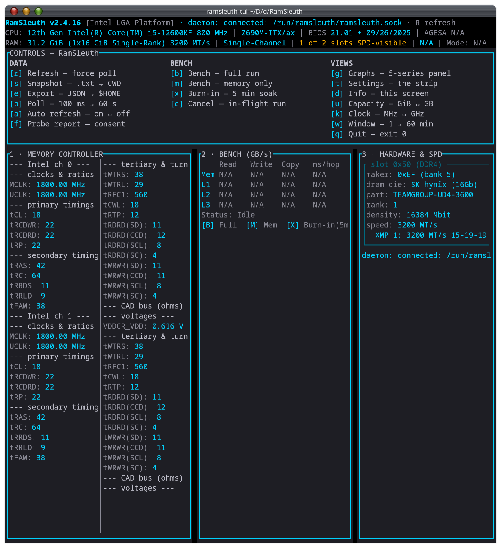
Another small catch while reading the probe-report again, it doubles what it reads as MCLK and reports that as MT/s. So it thinks my 3600 “MHz” (1800Mhz, 3600MT/s) DDR4 is running at 7200MT/s.
1 Like

I mean, I couldn’t ask for better feedback! Thank you! Holy cow, you’ve gone out of your way with what you’ve provided me here, thank you so much.

Aside from some very glaringly obvious issues I see this morning with coffee in hand, you’re probe report and hexdump is invaluable! (I’ll be honest, I totally have ignored the tui for the last couple releases and was considering scraping it)

Thank you again for taking your time to provide such awesome info. I’ll post up a new release once I can wrap my head around some more of this.

1 Like

2.4.16

The headline: Intel readouts — dual-channel hopefully resolve correctly and the memory-speed readout (no more doubled MT/s).

Also in this one:

Memory & Latency Benchmark — measures each tier (DRAM + L1/L2/L3) honestly, with a fast latency pass.
Wider AMD coverage — Zen 4/5 and now decode fully.
Consistent numbers across the TUI, GUI, and CLI (now single source).
TUI polish / update — cleaner graph, readable probe report, live burn-in timer.

A lot more still in the works, but these changes will hopefully get intel functional.

1 Like

Seen that you have been busy ………

My pleasure! I used to be massively into overclocking (I liked X chipsets with Xeons/i7s/i9s, had to OC to get good gaming performance) and the lack of good utilities for benching and voltage monitoring on Linux has always sucked. I’ve got LACT for the GPU side now (close enough to MSI Afterburner), OCCT does fine for stress tests, but it doesn’t monitor voltages. Thus I’m super happy to see a utility like this that’ll cover the AIDA64-like RAM benching and fold in voltage monitoring too. I really like TUIs for monitoring utilities so I’m glad you decided to keep that.

I’ll give it a spin when I get home tonight, and re-run the probe to see if the output is correct this time around.

1 Like

New probe:

2.4.16 probe

RamSleuth Probe Report

12th Gen Intel(R) Core™ i5-12600KF — Alder Lake on linux (kernel 7.3.0-rc6-tkg-bore-llvm), RamSleuth v2.4.16

System

Field Value
CPU 12th Gen Intel(R) Core™ i5-12600KF
Vendor Intel
Generation Alder Lake
PCI Host Bridge 0x4648
Kernel 7.3.0-rc6-tkg-bore-llvm
OS linux
Arch x86_64
RamSleuth Version 2.4.16
Telemetry Source dev-mem

Decoded Telemetry

CPU

Field Value
vendor Intel AlderLake
brand 12th Gen Intel(R) Core™ i5-12600KF
CPU Core Voltage 0.768 V

AMD

N/A (unsupported hardware)

Intel

Field Value
channel mode Single-Channel

Channel 0

Clock Value
MCLK 1800.00 MHz
MT/s 3600 MT/s
UCLK 1800.00 MHz
FCLK N/A (not applicable)
UCLK:MCLK N/A (not applicable)
gear mode 1x
GDM N/A (not applicable)
PDM N/A (not applicable)
command rate N/A (not applicable)
Timing (ticks) Value
tCL N/A (parse error: tCL 0 ticks outside plausible range [1, 2048])
tRCDWR 2
tRCDRD 2
tRP 8
tRAS N/A (parse error: tRAS 0 ticks outside plausible range [1, 2048])
tRC N/A (not applicable)
tRRDS 4
tRRLD N/A (parse error: tRRD_L 0 ticks outside plausible range [1, 2048])
tFAW N/A (parse error: tFAW 0 ticks outside plausible range [1, 2048])
tWTRS 26
tWTRL 2
tWR N/A (parse error: tWR 0 ticks outside plausible range [1, 2048])
tRFC1 1024
tRFC2 N/A (not applicable)
tRFCsb N/A (parse error: tRFCsb 0 ticks outside plausible range [1, 2048])
tCWL 1
tRTP 1
tRDWR N/A (not applicable)
tWRRD N/A (not applicable)
tRDRD(SD) N/A (parse error: tRDRD(dr) 0 ticks outside plausible range [1, 2048])
tRDRD(CCD) N/A (parse error: tRDRD(dd) 0 ticks outside plausible range [1, 2048])
tRDRD(SCL) N/A (parse error: tRDRD(sg) 0 ticks outside plausible range [1, 2048])
tRDRD(SC) N/A (parse error: tRDRD(dg) 0 ticks outside plausible range [1, 2048])
tWRWR(SD) N/A (not applicable)
tWRWR(CCD) N/A (not applicable)
tWRWR(SCL) N/A (parse error: tWRWR(sg) 0 ticks outside plausible range [1, 2048])
tWRWR(SC) N/A (parse error: tWRWR(dg) 0 ticks outside plausible range [1, 2048])
CAD bus (ohms) Value
proc ODT N/A (not applicable)
RTT nom N/A (not applicable)
RTT wr N/A (not applicable)
RTT park N/A (not applicable)
CLK drive N/A (not applicable)
ADD/CMD drive N/A (not applicable)
CS/ODT drive N/A (not applicable)
CKE drive N/A (not applicable)
Rail (V) Value
VDDCR_SOC N/A (not applicable)
VDDIO_MEM N/A (not applicable)
VDD_MISC N/A (not applicable)
VPP N/A (not applicable)
RTL (ticks) Value
RTL N/A (not applicable)

Channel 1

Clock Value
MCLK 1800.00 MHz
MT/s 3600 MT/s
UCLK 1800.00 MHz
FCLK N/A (not applicable)
UCLK:MCLK N/A (not applicable)
gear mode 1x
GDM N/A (not applicable)
PDM N/A (not applicable)
command rate N/A (not applicable)
Timing (ticks) Value
tCL N/A (parse error: tCL: register read failed)
tRCDWR N/A (parse error: tRCD: register read failed)
tRCDRD N/A (parse error: tRCD: register read failed)
tRP N/A (parse error: tRP: register read failed)
tRAS N/A (parse error: tRAS: register read failed)
tRC N/A (not applicable)
tRRDS N/A (parse error: tRRD_S: register read failed)
tRRLD N/A (parse error: tRRD_L: register read failed)
tFAW N/A (parse error: tFAW: register read failed)
tWTRS N/A (parse error: tWTR_S: register read failed)
tWTRL N/A (parse error: tWTR_L: register read failed)
tWR N/A (parse error: tWR: register read failed)
tRFC1 N/A (parse error: tRFC1: register read failed)
tRFC2 N/A (not applicable)
tRFCsb N/A (parse error: tRFCsb: register read failed)
tCWL N/A (parse error: tCWL: register read failed)
tRTP N/A (parse error: tRTP: register read failed)
tRDWR N/A (not applicable)
tWRRD N/A (not applicable)
tRDRD(SD) N/A (parse error: tRDRD(dr): register read failed)
tRDRD(CCD) N/A (parse error: tRDRD(dd): register read failed)
tRDRD(SCL) N/A (parse error: tRDRD(sg): register read failed)
tRDRD(SC) N/A (parse error: tRDRD(dg): register read failed)
tWRWR(SD) N/A (not applicable)
tWRWR(CCD) N/A (not applicable)
tWRWR(SCL) N/A (parse error: tWRWR(sg): register read failed)
tWRWR(SC) N/A (parse error: tWRWR(dg): register read failed)
CAD bus (ohms) Value
proc ODT N/A (not applicable)
RTT nom N/A (not applicable)
RTT wr N/A (not applicable)
RTT park N/A (not applicable)
CLK drive N/A (not applicable)
ADD/CMD drive N/A (not applicable)
CS/ODT drive N/A (not applicable)
CKE drive N/A (not applicable)
Rail (V) Value
VDDCR_SOC N/A (not applicable)
VDDIO_MEM N/A (not applicable)
VDD_MISC N/A (not applicable)
VPP N/A (not applicable)
RTL (ticks) Value
RTL N/A (not applicable)

Channel 2

Clock Value
MCLK 1800.00 MHz
MT/s 3600 MT/s
UCLK 1800.00 MHz
FCLK N/A (not applicable)
UCLK:MCLK N/A (not applicable)
gear mode 1x
GDM N/A (not applicable)
PDM N/A (not applicable)
command rate N/A (not applicable)
Timing (ticks) Value
tCL N/A (parse error: tCL 0 ticks outside plausible range [1, 2048])
tRCDWR N/A (parse error: tRCD 0 ticks outside plausible range [1, 2048])
tRCDRD N/A (parse error: tRCD 0 ticks outside plausible range [1, 2048])
tRP N/A (parse error: tRP 0 ticks outside plausible range [1, 2048])
tRAS N/A (parse error: tRAS 0 ticks outside plausible range [1, 2048])
tRC N/A (not applicable)
tRRDS 1
tRRLD N/A (parse error: tRRD_L 0 ticks outside plausible range [1, 2048])
tFAW N/A (parse error: tFAW 0 ticks outside plausible range [1, 2048])
tWTRS N/A (parse error: tWTR_S 0 ticks outside plausible range [1, 2048])
tWTRL 24
tWR N/A (parse error: tWR 0 ticks outside plausible range [1, 2048])
tRFC1 N/A (parse error: tRFC1 0 ticks outside plausible range [1, 2048])
tRFC2 N/A (not applicable)
tRFCsb N/A (parse error: tRFCsb 0 ticks outside plausible range [1, 2048])
tCWL 16
tRTP 16
tRDWR N/A (not applicable)
tWRRD N/A (not applicable)
tRDRD(SD) N/A (parse error: tRDRD(dr) 0 ticks outside plausible range [1, 2048])
tRDRD(CCD) N/A (parse error: tRDRD(dd) 0 ticks outside plausible range [1, 2048])
tRDRD(SCL) N/A (parse error: tRDRD(sg) 0 ticks outside plausible range [1, 2048])
tRDRD(SC) N/A (parse error: tRDRD(dg) 0 ticks outside plausible range [1, 2048])
tWRWR(SD) N/A (not applicable)
tWRWR(CCD) N/A (not applicable)
tWRWR(SCL) N/A (parse error: tWRWR(sg) 0 ticks outside plausible range [1, 2048])
tWRWR(SC) N/A (parse error: tWRWR(dg) 0 ticks outside plausible range [1, 2048])
CAD bus (ohms) Value
proc ODT N/A (not applicable)
RTT nom N/A (not applicable)
RTT wr N/A (not applicable)
RTT park N/A (not applicable)
CLK drive N/A (not applicable)
ADD/CMD drive N/A (not applicable)
CS/ODT drive N/A (not applicable)
CKE drive N/A (not applicable)
Rail (V) Value
VDDCR_SOC N/A (not applicable)
VDDIO_MEM N/A (not applicable)
VDD_MISC N/A (not applicable)
VPP N/A (not applicable)
RTL (ticks) Value
RTL N/A (not applicable)

Channel 3

Clock Value
MCLK 1800.00 MHz
MT/s 3600 MT/s
UCLK 1800.00 MHz
FCLK N/A (not applicable)
UCLK:MCLK N/A (not applicable)
gear mode 1x
GDM N/A (not applicable)
PDM N/A (not applicable)
command rate N/A (not applicable)
Timing (ticks) Value
tCL N/A (parse error: tCL: register read failed)
tRCDWR N/A (parse error: tRCD: register read failed)
tRCDRD N/A (parse error: tRCD: register read failed)
tRP N/A (parse error: tRP: register read failed)
tRAS N/A (parse error: tRAS: register read failed)
tRC N/A (not applicable)
tRRDS N/A (parse error: tRRD_S: register read failed)
tRRLD N/A (parse error: tRRD_L: register read failed)
tFAW N/A (parse error: tFAW: register read failed)
tWTRS N/A (parse error: tWTR_S: register read failed)
tWTRL N/A (parse error: tWTR_L: register read failed)
tWR N/A (parse error: tWR: register read failed)
tRFC1 N/A (parse error: tRFC1: register read failed)
tRFC2 N/A (not applicable)
tRFCsb N/A (parse error: tRFCsb: register read failed)
tCWL N/A (parse error: tCWL: register read failed)
tRTP N/A (parse error: tRTP: register read failed)
tRDWR N/A (not applicable)
tWRRD N/A (not applicable)
tRDRD(SD) N/A (parse error: tRDRD(dr): register read failed)
tRDRD(CCD) N/A (parse error: tRDRD(dd): register read failed)
tRDRD(SCL) N/A (parse error: tRDRD(sg): register read failed)
tRDRD(SC) N/A (parse error: tRDRD(dg): register read failed)
tWRWR(SD) N/A (not applicable)
tWRWR(CCD) N/A (not applicable)
tWRWR(SCL) N/A (parse error: tWRWR(sg): register read failed)
tWRWR(SC) N/A (parse error: tWRWR(dg): register read failed)
CAD bus (ohms) Value
proc ODT N/A (not applicable)
RTT nom N/A (not applicable)
RTT wr N/A (not applicable)
RTT park N/A (not applicable)
CLK drive N/A (not applicable)
ADD/CMD drive N/A (not applicable)
CS/ODT drive N/A (not applicable)
CKE drive N/A (not applicable)
Rail (V) Value
VDDCR_SOC N/A (not applicable)
VDDIO_MEM N/A (not applicable)
VDD_MISC N/A (not applicable)
VPP N/A (not applicable)
RTL (ticks) Value
RTL N/A (not applicable)

SPD

Module 0x50 (DDR4)

Field Value
maker 0xEF (bank 5)
die maker SK hynix
die type N/A (not applicable)
devices 8
part TEAMGROUP-UD4-3600
serial 0104D817
rank 1
density 16384 Mbit
speed 3200 MT/s
  • profile 1 (XMP): 3200 MT/s, 15-19-19-37 @ 1.350 V

Platform

Field Value
CPU clock (MHz) 867.16 MHz
motherboard Z690M-ITX/ax
BIOS 21.01 + 09/26/2025
AGESA N/A (not applicable)
SMU version N/A (not applicable)
total capacity 31.2 GiB
per-DIMM sizes 16.0 GiB

Raw Registers

Register Value
MC_BIOS_REQ 0x79E00124
TC_CH0_DBP 0xFFFFFFFF
TC_CH0_RAP 0xFFFFFFFF
TC_CH0_RFP 0xFFFFFFFF
TC_CH0_RAP2 0xFFFFFFFF
TC_CH0_RDRD 0xFFFFFFFF
TC_CH0_RDWR 0xFFFFFFFF
TC_CH0_WRRD 0xFFFFFFFF
TC_CH0_WRWR 0xFFFFFFFF
TC_CH1_DBP 0xFFFFFFFF
TC_CH1_RAP 0xFFFFFFFF
TC_CH1_RFP 0xFFFFFFFF
TC_CH1_RAP2 0xFFFFFFFF
TC_CH1_RDRD 0xFFFFFFFF
TC_CH1_RDWR 0xFFFFFFFF
TC_CH1_WRRD 0xFFFFFFFF
TC_CH1_WRWR 0xFFFFFFFF
TC_CH2_DBP 0xFFFFFFFF
TC_CH2_RAP 0xFFFFFFFF
TC_CH2_RFP 0xFFFFFFFF
TC_CH2_RAP2 0xFFFFFFFF
TC_CH2_RDRD 0xFFFFFFFF
TC_CH2_RDWR 0xFFFFFFFF
TC_CH2_WRRD 0xFFFFFFFF
TC_CH2_WRWR 0xFFFFFFFF
TC_CH3_DBP 0xFFFFFFFF
TC_CH3_RAP 0xFFFFFFFF
TC_CH3_RFP 0xFFFFFFFF
TC_CH3_RAP2 0xFFFFFFFF
TC_CH3_RDRD 0xFFFFFFFF
TC_CH3_RDWR 0xFFFFFFFF
TC_CH3_WRRD 0xFFFFFFFF
TC_CH3_WRWR 0xFFFFFFFF
MCL0_PRE 0x01000208
MCL0_ACT 0x00000400
MCL0_ACT2 0xFFFFFFFF
MCL0_WTR 0x0100021A
MCL0_RFP 0x00000400
MCL0_RFP2 0x00000000
MCL0_RDRD 0x00000000
MCL0_WRWR 0x00620000
MCL1_PRE 0x10000000
MCL1_ACT 0x00000100
MCL1_ACT2 0x00000000
MCL1_WTR 0x10001800
MCL1_RFP 0x00000000
MCL1_RFP2 0x00000000
MCL1_RDRD 0x00000000
MCL1_WRWR 0x00000000
MAD_INTER_CHANNEL N/A (absent)
MAD_INTRA_CH0 N/A (absent)
MAD_INTRA_CH1 N/A (absent)
MAD_DIMM_CH0 N/A (absent)
MAD_DIMM_CH1 N/A (absent)
MAD_DIMM_CH2 N/A (absent)
MAD_DIMM_CH3 N/A (absent)
MCHBAR_BASE 0xFEDC0000
MCHBAR_ENABLED true

N/A Reasons

  • amd (whole branch) — N/A (unsupported hardware)
  • intel.ch0.clocks.fclk — N/A (not applicable)
  • intel.ch0.clocks.div_mode — N/A (not applicable)
  • intel.ch0.clocks.gdm — N/A (not applicable)
  • intel.ch0.clocks.pdm — N/A (not applicable)
  • intel.ch0.clocks.command_rate — N/A (not applicable)
  • intel.ch0.timings.cl — N/A (parse error: tCL 0 ticks outside plausible range [1, 2048])
  • intel.ch0.timings.ras — N/A (parse error: tRAS 0 ticks outside plausible range [1, 2048])
  • intel.ch0.timings.rc — N/A (not applicable)
  • intel.ch0.timings.rrld — N/A (parse error: tRRD_L 0 ticks outside plausible range [1, 2048])
  • intel.ch0.timings.faw — N/A (parse error: tFAW 0 ticks outside plausible range [1, 2048])
  • intel.ch0.timings.wr — N/A (parse error: tWR 0 ticks outside plausible range [1, 2048])
  • intel.ch0.timings.rfc2 — N/A (not applicable)
  • intel.ch0.timings.rfcsb — N/A (parse error: tRFCsb 0 ticks outside plausible range [1, 2048])
  • intel.ch0.timings.rdwr — N/A (not applicable)
  • intel.ch0.timings.wrrd — N/A (not applicable)
  • intel.ch0.timings.rdrd_sd — N/A (parse error: tRDRD(dr) 0 ticks outside plausible range [1, 2048])
  • intel.ch0.timings.rdrd_dd — N/A (parse error: tRDRD(dd) 0 ticks outside plausible range [1, 2048])
  • intel.ch0.timings.rdrd_scl — N/A (parse error: tRDRD(sg) 0 ticks outside plausible range [1, 2048])
  • intel.ch0.timings.rdrd_sc — N/A (parse error: tRDRD(dg) 0 ticks outside plausible range [1, 2048])
  • intel.ch0.timings.wrwr_sd — N/A (not applicable)
  • intel.ch0.timings.wrwr_dd — N/A (not applicable)
  • intel.ch0.timings.wrwr_scl — N/A (parse error: tWRWR(sg) 0 ticks outside plausible range [1, 2048])
  • intel.ch0.timings.wrwr_sc — N/A (parse error: tWRWR(dg) 0 ticks outside plausible range [1, 2048])
  • intel.ch0.cad_bus.proc_odt — N/A (not applicable)
  • intel.ch0.cad_bus.rtt_nom — N/A (not applicable)
  • intel.ch0.cad_bus.rtt_wr — N/A (not applicable)
  • intel.ch0.cad_bus.rtt_park — N/A (not applicable)
  • intel.ch0.cad_bus.clk_drv — N/A (not applicable)
  • intel.ch0.cad_bus.addr_cmd_drv — N/A (not applicable)
  • intel.ch0.cad_bus.cs_odt_drv — N/A (not applicable)
  • intel.ch0.cad_bus.cke_drv — N/A (not applicable)
  • intel.ch0.voltages.vddcr_soc — N/A (not applicable)
  • intel.ch0.voltages.vddio_mem — N/A (not applicable)
  • intel.ch0.voltages.vdd_misc — N/A (not applicable)
  • intel.ch0.voltages.vpp — N/A (not applicable)
  • intel.ch0.rtl — N/A (not applicable)
  • intel.ch1.clocks.fclk — N/A (not applicable)
  • intel.ch1.clocks.div_mode — N/A (not applicable)
  • intel.ch1.clocks.gdm — N/A (not applicable)
  • intel.ch1.clocks.pdm — N/A (not applicable)
  • intel.ch1.clocks.command_rate — N/A (not applicable)
  • intel.ch1.timings.cl — N/A (parse error: tCL: register read failed)
  • intel.ch1.timings.rcwdwr — N/A (parse error: tRCD: register read failed)
  • intel.ch1.timings.rcdrd — N/A (parse error: tRCD: register read failed)
  • intel.ch1.timings.rp — N/A (parse error: tRP: register read failed)
  • intel.ch1.timings.ras — N/A (parse error: tRAS: register read failed)
  • intel.ch1.timings.rc — N/A (not applicable)
  • intel.ch1.timings.rrds — N/A (parse error: tRRD_S: register read failed)
  • intel.ch1.timings.rrld — N/A (parse error: tRRD_L: register read failed)
  • intel.ch1.timings.faw — N/A (parse error: tFAW: register read failed)
  • intel.ch1.timings.wtrs — N/A (parse error: tWTR_S: register read failed)
  • intel.ch1.timings.wtrl — N/A (parse error: tWTR_L: register read failed)
  • intel.ch1.timings.wr — N/A (parse error: tWR: register read failed)
  • intel.ch1.timings.rfc1 — N/A (parse error: tRFC1: register read failed)
  • intel.ch1.timings.rfc2 — N/A (not applicable)
  • intel.ch1.timings.rfcsb — N/A (parse error: tRFCsb: register read failed)
  • intel.ch1.timings.cwl — N/A (parse error: tCWL: register read failed)
  • intel.ch1.timings.rtp — N/A (parse error: tRTP: register read failed)
  • intel.ch1.timings.rdwr — N/A (not applicable)
  • intel.ch1.timings.wrrd — N/A (not applicable)
  • intel.ch1.timings.rdrd_sd — N/A (parse error: tRDRD(dr): register read failed)
  • intel.ch1.timings.rdrd_dd — N/A (parse error: tRDRD(dd): register read failed)
  • intel.ch1.timings.rdrd_scl — N/A (parse error: tRDRD(sg): register read failed)
  • intel.ch1.timings.rdrd_sc — N/A (parse error: tRDRD(dg): register read failed)
  • intel.ch1.timings.wrwr_sd — N/A (not applicable)
  • intel.ch1.timings.wrwr_dd — N/A (not applicable)
  • intel.ch1.timings.wrwr_scl — N/A (parse error: tWRWR(sg): register read failed)
  • intel.ch1.timings.wrwr_sc — N/A (parse error: tWRWR(dg): register read failed)
  • intel.ch1.cad_bus.proc_odt — N/A (not applicable)
  • intel.ch1.cad_bus.rtt_nom — N/A (not applicable)
  • intel.ch1.cad_bus.rtt_wr — N/A (not applicable)
  • intel.ch1.cad_bus.rtt_park — N/A (not applicable)
  • intel.ch1.cad_bus.clk_drv — N/A (not applicable)
  • intel.ch1.cad_bus.addr_cmd_drv — N/A (not applicable)
  • intel.ch1.cad_bus.cs_odt_drv — N/A (not applicable)
  • intel.ch1.cad_bus.cke_drv — N/A (not applicable)
  • intel.ch1.voltages.vddcr_soc — N/A (not applicable)
  • intel.ch1.voltages.vddio_mem — N/A (not applicable)
  • intel.ch1.voltages.vdd_misc — N/A (not applicable)
  • intel.ch1.voltages.vpp — N/A (not applicable)
  • intel.ch1.rtl — N/A (not applicable)
  • intel.ch2.clocks.fclk — N/A (not applicable)
  • intel.ch2.clocks.div_mode — N/A (not applicable)
  • intel.ch2.clocks.gdm — N/A (not applicable)
  • intel.ch2.clocks.pdm — N/A (not applicable)
  • intel.ch2.clocks.command_rate — N/A (not applicable)
  • intel.ch2.timings.cl — N/A (parse error: tCL 0 ticks outside plausible range [1, 2048])
  • intel.ch2.timings.rcwdwr — N/A (parse error: tRCD 0 ticks outside plausible range [1, 2048])
  • intel.ch2.timings.rcdrd — N/A (parse error: tRCD 0 ticks outside plausible range [1, 2048])
  • intel.ch2.timings.rp — N/A (parse error: tRP 0 ticks outside plausible range [1, 2048])
  • intel.ch2.timings.ras — N/A (parse error: tRAS 0 ticks outside plausible range [1, 2048])
  • intel.ch2.timings.rc — N/A (not applicable)
  • intel.ch2.timings.rrld — N/A (parse error: tRRD_L 0 ticks outside plausible range [1, 2048])
  • intel.ch2.timings.faw — N/A (parse error: tFAW 0 ticks outside plausible range [1, 2048])
  • intel.ch2.timings.wtrs — N/A (parse error: tWTR_S 0 ticks outside plausible range [1, 2048])
  • intel.ch2.timings.wr — N/A (parse error: tWR 0 ticks outside plausible range [1, 2048])
  • intel.ch2.timings.rfc1 — N/A (parse error: tRFC1 0 ticks outside plausible range [1, 2048])
  • intel.ch2.timings.rfc2 — N/A (not applicable)
  • intel.ch2.timings.rfcsb — N/A (parse error: tRFCsb 0 ticks outside plausible range [1, 2048])
  • intel.ch2.timings.rdwr — N/A (not applicable)
  • intel.ch2.timings.wrrd — N/A (not applicable)
  • intel.ch2.timings.rdrd_sd — N/A (parse error: tRDRD(dr) 0 ticks outside plausible range [1, 2048])
  • intel.ch2.timings.rdrd_dd — N/A (parse error: tRDRD(dd) 0 ticks outside plausible range [1, 2048])
  • intel.ch2.timings.rdrd_scl — N/A (parse error: tRDRD(sg) 0 ticks outside plausible range [1, 2048])
  • intel.ch2.timings.rdrd_sc — N/A (parse error: tRDRD(dg) 0 ticks outside plausible range [1, 2048])
  • intel.ch2.timings.wrwr_sd — N/A (not applicable)
  • intel.ch2.timings.wrwr_dd — N/A (not applicable)
  • intel.ch2.timings.wrwr_scl — N/A (parse error: tWRWR(sg) 0 ticks outside plausible range [1, 2048])
  • intel.ch2.timings.wrwr_sc — N/A (parse error: tWRWR(dg) 0 ticks outside plausible range [1, 2048])
  • intel.ch2.cad_bus.proc_odt — N/A (not applicable)
  • intel.ch2.cad_bus.rtt_nom — N/A (not applicable)
  • intel.ch2.cad_bus.rtt_wr — N/A (not applicable)
  • intel.ch2.cad_bus.rtt_park — N/A (not applicable)
  • intel.ch2.cad_bus.clk_drv — N/A (not applicable)
  • intel.ch2.cad_bus.addr_cmd_drv — N/A (not applicable)
  • intel.ch2.cad_bus.cs_odt_drv — N/A (not applicable)
  • intel.ch2.cad_bus.cke_drv — N/A (not applicable)
  • intel.ch2.voltages.vddcr_soc — N/A (not applicable)
  • intel.ch2.voltages.vddio_mem — N/A (not applicable)
  • intel.ch2.voltages.vdd_misc — N/A (not applicable)
  • intel.ch2.voltages.vpp — N/A (not applicable)
  • intel.ch2.rtl — N/A (not applicable)
  • intel.ch3.clocks.fclk — N/A (not applicable)
  • intel.ch3.clocks.div_mode — N/A (not applicable)
  • intel.ch3.clocks.gdm — N/A (not applicable)
  • intel.ch3.clocks.pdm — N/A (not applicable)
  • intel.ch3.clocks.command_rate — N/A (not applicable)
  • intel.ch3.timings.cl — N/A (parse error: tCL: register read failed)
  • intel.ch3.timings.rcwdwr — N/A (parse error: tRCD: register read failed)
  • intel.ch3.timings.rcdrd — N/A (parse error: tRCD: register read failed)
  • intel.ch3.timings.rp — N/A (parse error: tRP: register read failed)
  • intel.ch3.timings.ras — N/A (parse error: tRAS: register read failed)
  • intel.ch3.timings.rc — N/A (not applicable)
  • intel.ch3.timings.rrds — N/A (parse error: tRRD_S: register read failed)
  • intel.ch3.timings.rrld — N/A (parse error: tRRD_L: register read failed)
  • intel.ch3.timings.faw — N/A (parse error: tFAW: register read failed)
  • intel.ch3.timings.wtrs — N/A (parse error: tWTR_S: register read failed)
  • intel.ch3.timings.wtrl — N/A (parse error: tWTR_L: register read failed)
  • intel.ch3.timings.wr — N/A (parse error: tWR: register read failed)
  • intel.ch3.timings.rfc1 — N/A (parse error: tRFC1: register read failed)
  • intel.ch3.timings.rfc2 — N/A (not applicable)
  • intel.ch3.timings.rfcsb — N/A (parse error: tRFCsb: register read failed)
  • intel.ch3.timings.cwl — N/A (parse error: tCWL: register read failed)
  • intel.ch3.timings.rtp — N/A (parse error: tRTP: register read failed)
  • intel.ch3.timings.rdwr — N/A (not applicable)
  • intel.ch3.timings.wrrd — N/A (not applicable)
  • intel.ch3.timings.rdrd_sd — N/A (parse error: tRDRD(dr): register read failed)
  • intel.ch3.timings.rdrd_dd — N/A (parse error: tRDRD(dd): register read failed)
  • intel.ch3.timings.rdrd_scl — N/A (parse error: tRDRD(sg): register read failed)
  • intel.ch3.timings.rdrd_sc — N/A (parse error: tRDRD(dg): register read failed)
  • intel.ch3.timings.wrwr_sd — N/A (not applicable)
  • intel.ch3.timings.wrwr_dd — N/A (not applicable)
  • intel.ch3.timings.wrwr_scl — N/A (parse error: tWRWR(sg): register read failed)
  • intel.ch3.timings.wrwr_sc — N/A (parse error: tWRWR(dg): register read failed)
  • intel.ch3.cad_bus.proc_odt — N/A (not applicable)
  • intel.ch3.cad_bus.rtt_nom — N/A (not applicable)
  • intel.ch3.cad_bus.rtt_wr — N/A (not applicable)
  • intel.ch3.cad_bus.rtt_park — N/A (not applicable)
  • intel.ch3.cad_bus.clk_drv — N/A (not applicable)
  • intel.ch3.cad_bus.addr_cmd_drv — N/A (not applicable)
  • intel.ch3.cad_bus.cs_odt_drv — N/A (not applicable)
  • intel.ch3.cad_bus.cke_drv — N/A (not applicable)
  • intel.ch3.voltages.vddcr_soc — N/A (not applicable)
  • intel.ch3.voltages.vddio_mem — N/A (not applicable)
  • intel.ch3.voltages.vdd_misc — N/A (not applicable)
  • intel.ch3.voltages.vpp — N/A (not applicable)
  • intel.ch3.rtl — N/A (not applicable)
  • spd[0x50].die_type — N/A (not applicable)
  • platform.agesa — N/A (not applicable)
  • platform.smu_version — N/A (not applicable)
  • raw.mad_inter_channel — N/A (register absent / read failed)
  • raw.mad_intra_ch0 — N/A (register absent / read failed)
  • raw.mad_intra_ch1 — N/A (register absent / read failed)
  • raw.mad_dimm_ch0 — N/A (register absent / read failed)
  • raw.mad_dimm_ch1 — N/A (register absent / read failed)
  • raw.mad_dimm_ch2 — N/A (register absent / read failed)
  • raw.mad_dimm_ch3 — N/A (register absent / read failed)

This report was auto-generated by RamSleuth v2.4.16. It contains no personal information (no username, hostname, IP, MAC, or serial numbers).

It’s reporting correct MT/s. The live view of the burn-in runs is real nice as well, same with the graphing fix.

It still reads single-channel, but that seems to be the override not being set up to fire (or just not firing correctly) when there’s two dimms. My motherboard seems to just… not expose a second DIMM’s SPD info, only the main one. The TUI correctly reads two channels though, it’s just the SPD section that’s bothered by the motherboard limitation (it also doesn’t read the 3600Mhz XMP profile, just the 3200MHz one).

Digging into this more with DeepSeek… I’m not getting the timings read properly because RamSlueth is using the DDR5 registers. Here’s the Intel 12th gen datasheet: https://www.intel.com/content/www/us/en/content-details/710723/12th-generation-intel-core-processors-datasheet-volume-2-of-2.html and direct link to the PDF (it’s massive): https://cdrdv2-public.intel.com/710723/710723-003.pdf. Pages ~114-116 have the MCHBAR register summary (and 116-187 the detail), and note that A) these chips have 2 memory controllers and B) with DDR4 it’s one channel per controller. That explains why it was reporting Controller 0/1 but Channel A on both. Here’s DeepSeek’s rip out of the relevant ones and what they map to:

12th gen ddr4 MCHBAR

Intel Alder Lake DDR4 MCHBAR timing registers

Source: Intel 12th Gen Core Datasheet Vol 2 (doc 710723-003), §3.2.66–3.2.87.
All offsets are MC0 / channel 0 and relative to the MCHBAR base.
MC0 ch1 = +0x800, MC0 broadcast = +0x1000, MC1 = +0x10000.
DDR4 Alder = 2 memory controllers × 1 channel each (no subchannels).

Bit ranges are [hi:lo] (inclusive). “Range” is the datasheet’s supported range.

Register Offset Bits Field Decodes to Range
TC_PRE E000h [62:59] DERATING_EXT LPDDR derating 0–4 (0 for DDR)
TC_PRE E000h [58:51] TRCD tRCD — ACT→CAS same bank 8–59
TC_PRE E000h [50:42] TRAS tRAS — ACT→PRE same bank 28–136
TC_PRE E000h [41:32] TWRPRE tWRPRE — WR→PRE same bank 18–200
TC_PRE E000h [23:20] TPPD tPPD — PRE→PRE same rank (not DDR5) 4–7
TC_PRE E000h [19:13] TRDPRE tRDPRE — RD→PRE same bank 4–32
TC_PRE E000h [12:8] TRPAB_EXT LPDDR only (0 for DDR4) 0–6
TC_PRE E000h [7:0] TRP tRP — PRE→ACT same bank 8–60
TC_ACT E008h [31:24] TREFSBRD tREFSBRD — refsb→ACT —
TC_ACT E008h [21:15] TRRD_DG tRRD_DG — ACT→ACT diff bank group 4–32
TC_ACT E008h [14:9] TRRD_SG tRRD_SG — ACT→ACT same bank group (tRRD_L for DDR4) 4–32
TC_ACT E008h [8:0] TFAW tFAW — four-activate window 16–88
TC_RDRD E00Ch [31:24] TRDRD_DD tRDRD_dd — RD→RD other DIMM 4–54
TC_RDRD E00Ch [23:16] TRDRD_DR tRDRD_dr — RD→RD other rank 4–54
TC_RDRD E00Ch [14:8] TRDRD_DG tRDRD_dg — RD→RD diff bank group 4–54
TC_RDRD E00Ch [7] ALLOW_2CYC_B2B_LPDDR LPDDR only —
TC_RDRD E00Ch [6:0] TRDRD_SG tRDRD_sg — RD→RD same bank group 4–54
TC_RDWR E010h [31:24] TRDWR_DD tRDWR_dd — RD→WR other DIMM 4–54
TC_RDWR E010h [23:16] TRDWR_DR tRDWR_dr — RD→WR other rank 4–54
TC_RDWR E010h [15:8] TRDWR_DG tRDWR_dg — RD→WR diff bank group 4–54
TC_RDWR E010h [7:0] TRDWR_SG tRDWR_sg — RD→WR same bank group 4–54
TC_WRRD E014h [31:25] TWRRD_DD tWRRD_dd — WR→RD other DIMM 4–54
TC_WRRD E014h [24:18] TWRRD_DR tWRRD_dr — WR→RD other rank 4–54
TC_WRRD E014h [17:9] TWRRD_DG tWRRD_dg — WR→RD diff bank group 4–65
TC_WRRD E014h [8:0] TWRRD_SG tWRRD_sg — WR→RD same bank group 4–145
TC_WRWR E018h [31:24] TWRWR_DD tWRWR_dd — WR→WR other DIMM 4–54
TC_WRWR E018h [22:16] TWRWR_DR tWRWR_dr — WR→WR other rank 4–54
TC_WRWR E018h [14:8] TWRWR_DG tWRWR_dg — WR→WR diff bank group 4–54
TC_WRWR E018h [6:0] TWRWR_SG tWRWR_sg — WR→WR same bank group 4–54
SC_ROUNDTRIP_LATENCY E020h [7:0] RANK_0_LATENCY read round-trip, rank 0 19–120
SC_ROUNDTRIP_LATENCY E020h [15:8] RANK_1_LATENCY read round-trip, rank 1 19–120
SC_ROUNDTRIP_LATENCY E020h [23:16] RANK_2_LATENCY read round-trip, rank 2 19–120
SC_ROUNDTRIP_LATENCY E020h [31:24] RANK_3_LATENCY read round-trip, rank 3 19–120
SC_ROUNDTRIP_LATENCY E020h [39:32] RANK_4_LATENCY read round-trip, rank 4 19–120
SC_ROUNDTRIP_LATENCY E020h [47:40] RANK_5_LATENCY read round-trip, rank 5 19–120
SC_ROUNDTRIP_LATENCY E020h [55:48] RANK_6_LATENCY read round-trip, rank 6 19–120
SC_ROUNDTRIP_LATENCY E020h [63:56] RANK_7_LATENCY read round-trip, rank 7 19–120
TC_PWRDN E050h [63:59] TPRPDEN any CMD→PDE 1–
TC_PWRDN E050h [53:48] TCSL CS-low pulse on PD exit —
TC_PWRDN E050h [47:42] TCSH CS-high pulse on PD exit —
TC_PWRDN E050h [41:32] TWRPDEN WR→power-down 4–204
TC_PWRDN E050h [28:21] TRDPDEN RD→power-down 4–100
TC_PWRDN E050h [20:14] TXPDLL power-up→RD/WR (slow exit) 4–63
TC_PWRDN E050h [13:7] TXP power-up→any command 4–24
TC_PWRDN E050h [6:0] TCKE tCKE — PD→PU min delay 4–24
TC_ODT E070h [31:24] TCWL tCWL — WR command→data (DDR4 min 5) 4–64
TC_ODT E070h [22:16] TCL tCL — RD command→data 4–72
TC_RFP E438h [31:24] TREFIX9 tREFI×9, in 1024-DCLK units (8*tREFI/1024) —
TC_RFP E438h [23:20] RAISE_BLK_WAIT refresh FSM block wait —
TC_RFP E438h [19:18] SRX_REF_DEBITS refreshes on SR exit —
TC_RFP E438h [17] HPREFONMRS HP refresh on MRS —
TC_RFP E438h [16] COUNTTREFIWHILEREFENOFF keep tREFI counter on —
TC_RFP E438h [15:12] REFRESH_PANIC_WM panic threshold ≤9
TC_RFP E438h [11:8] REFRESH_HP_WM high-priority threshold —
TC_RFP E438h [7:0] OREF_RI rank-idle period (DCLK) —
TC_RFTP E43Ch [30:18] TRFC tRFC — refresh time default 180
TC_RFTP E43Ch [17:0] TREFI tREFI — avg refresh interval (tCK) default 4100
TC_SRFTP E440h [12:0] TXSDLL SR-exit→first data RD/WR —
MAD_INTER_CHANNEL D800h [31] HALFCACHELINEMODE 32 B cacheline mode —
MAD_INTER_CHANNEL D800h [28:27] CH_WIDTH 0=x16, 1=x32, 2=x64 —
MAD_INTER_CHANNEL D800h [19:12] CH_S_SIZE channel S size, ×0.5 GB 0–64 GB
MAD_INTER_CHANNEL D800h [4] CH_L_MAP channel L → physical channel 0/1
MAD_INTER_CHANNEL D800h [2:0] DDR_TYPE 0=DDR4, 1=DDR5, 2=LPDDR5, 3=LPDDR4 —

Access: BIOS RW, SMM R, OS R (read-only from userspace) for every register
above, so the timings are readable via MCHBAR MMIO.

Once the register reads are correct, it pulls the timings as normal:

Still reading as single-channel (in the probe) and 1x16GiB single DIMM in the UI, as well as only a single SPD exposure, and not reading the 3600MT/s XMP profile this kit does have. I’ll look more into it tomorrow. I’m thinking it’s a combination of my motherboard + something not reading right.

1 Like

Got sidetracked with some other projects, finally pointed DS back at this.

The XMP read miss is because XMP 2.0 has a timebase correction for tCK at +0x26 (sdramCycleTimeFc). RamSleuth already reads the equivalent for tRCD and tRP, it’s just not checking the tCK one. On my kit specifically, it’s a -69ps offset, bringing it to 556ps or ~3597MT/s. Here’s DeepSeek’s report:

DS Report on XMP tCK skip

XMP speed decode — why DDR4-3600 kits read as 3200

Symptom: the 3600 MHz XMP profile is not picked up — the decode reports 3200.
Cause: RamSleuth reads only half of the cycle-time field.

The XMP 2.0 profile stores tCK in two parts: a coarse value in MTB units
(125 ps each) plus a signed fine-timebase correction in ps that completes it:

tCK = (coarse_byte × 125) + fine_correction_ps

The code reads the coarse byte only and skips the correction. Both DDR4-3600
kits tested store coarse = 5 with a negative correction (−69 / −70 ps), i.e.
tCK ≈ 555–556 ps — the real 3600 value — but with the correction dropped it
reads 5 × 125 = 625 ps → 3200 MT/s.

Field locations in the 47-byte XMP 2.0 profile (offsets from the profile base):

  • +0x03 — coarse tCK in MTB (125 ps)
  • +0x26 — sdramCycleTimeFc, the signed fine correction in ps ← not read by RamSleuth
  • (RamSleuth does read the equivalent fine correction for tRCD at +0x24 and
    tRP at +0x23 — it just skips the one for tCK.)

What the two real kits store (verified byte-by-byte):

  • TEAMGROUP UD4-3600: +0x03 = 5, +0x26 = 0xBB (−69) → 556 ps → ~3597 MT/s
  • G.Skill F4-3600C18-32GVK: +0x03 = 5, +0x26 = 0xBA (−70) → 555 ps → ~3604 MT/s

Both are physically 3600 kits; with the correction applied the timings also land
on the published values (tRCD/tRP ≈ 22, tRAS ≈ 42 at ~555 ps).

Two things left to decide:

  1. The raw computed rate is 3597 / 3604, while both kits are sold as 3600 — so
    rounding / snapping to a standard rate may be wanted.
  2. The XMP CL bitmap is read as its lowest set bit, which gives CL15 on the
    TEAMGROUP kit (bitmap 0x1F = CL15–19) though it’s rated CL18 — worth a look.

References

  • XMP 2.0 profile layout (source for +0x26): integralfx/DDR4XMPEditor,
    DDR4SPD/XMP.cs — https://github.com/integralfx/DDR4XMPEditor/blob/master/DDR4SPD/XMP.cs
  • G.Skill F4-3600C18-32GVK raw SPD: the IMAGE_A_GSKILL 512-byte array
    already committed in crates/ramsleuth-telemetry/src/spd_decode.rs.
  • TEAMGROUP UD4-3600 raw SPD (512 B, live capture from the reporter’s
    hardware) — full dump below; XMP profile 1 spans 0x189..0x1B8, so +0x03 is
    byte 0x18C and +0x26 is byte 0x1AF.
000000  23 11 0c 02 86 29 00 08 00 60 00 03 01 03 00 00
000010  00 00 07 0d f8 0f 00 00 6b 6b 6b 11 00 6b 30 11
000020  f0 0a 20 08 00 a8 1b 28 28 00 00 00 00 00 00 00
000030  00 00 00 00 00 00 00 00 00 00 00 00 00 00 00 00
000040  00 00 00 00 00 00 00 00 00 00 00 00 00 00 00 00
000050  00 00 00 00 00 00 00 00 00 00 00 00 00 00 00 00
000060  00 00 00 00 00 00 00 00 00 00 00 00 00 00 00 00
000070  00 00 00 00 00 00 9c b5 c9 c9 c9 c9 00 d6 22 a3
000080  11 11 60 01 00 00 00 00 00 00 00 00 00 00 00 00
000090  00 00 00 00 00 00 00 00 00 00 00 00 00 00 00 00
0000a0  00 00 00 00 00 00 00 00 00 00 00 00 00 00 00 00
0000b0  00 00 00 00 00 00 00 00 00 00 00 00 00 00 00 00
0000c0  00 00 00 00 00 00 00 00 00 00 00 00 00 00 00 00
0000d0  00 00 00 00 00 00 00 00 00 00 00 00 00 00 00 00
0000e0  00 00 00 00 00 00 00 00 00 00 00 00 00 00 00 00
0000f0  00 00 00 00 00 00 00 00 00 00 00 00 00 00 ce 6c
000100  00 00 00 00 00 00 00 00 00 00 00 00 00 00 00 00
000110  00 00 00 00 00 00 00 00 00 00 00 00 00 00 00 00
000120  00 00 00 00 00 00 00 00 00 00 00 00 00 00 00 00
000130  00 00 00 00 00 00 00 00 00 00 00 00 00 00 00 00
000140  04 ef 00 23 21 01 04 d8 17 54 45 41 4d 47 52 4f
000150  55 50 2d 55 44 34 2d 33 36 30 30 20 20 00 80 ad
000160  ff 10 23 05 23 00 60 00 00 00 00 00 00 00 00 00
000170  00 00 00 00 00 00 00 00 00 00 00 00 00 00 00 00
000180  0c 4a 01 20 00 00 00 00 00 a3 00 00 05 00 1f 00
000190  00 50 62 62 10 ba 1c 30 11 f0 0a 20 08 00 a8 28
0001a0  28 00 00 00 00 00 00 00 00 00 00 00 90 90 00 bb
0001b0  00 00 00 00 00 00 00 00 00 00 00 00 00 00 00 00
0001c0  00 00 00 00 00 00 00 00 00 00 00 00 00 00 00 00
0001d0  00 00 00 00 00 00 00 00 00 00 00 00 00 00 00 00
0001e0  15 35 70 35 01 fe 04 27 21 32 36 30 36 01 00 00
0001f0  4d 42 35 35 30 00 00 50 00 00 15 02 01 22 01 00

Key bytes in XMP profile 1 (base 0x189):

0x18c  (+0x03) 05   coarse tCK = 5 MTB (625 ps)
0x192  (+0x09) 62   tRCD MTB = 98
0x193  (+0x0A) 62   tRP  MTB = 98
0x195  (+0x0C) ba   tRAS lo byte -> 186 MTB
0x1ac  (+0x23) 90   tRP  FTB = -112 ps
0x1ad  (+0x24) 90   tRCD FTB = -112 ps
0x1af  (+0x26) bb   tCK  FTB =  -69 ps  -> 5x125-69 = 556 ps -> ~3597 MT/s

The SPD issue is my motherboard, it only reports one DIMM. SMBIOS correctly sees two DIMMs, which is why they both show up in the timings section and the probe report. Switching the channel/DIMM size/count/rank to SMBIOS, or adding a guard that falls back to that if SPD fails (Ramsleuth correctly sees that I have 32GB RAM, so there only being 1x16GB DIMM should clue it in that SPD is failing) should fix it.

1 Like

Thanks for this awesome tool. I did some manual setup to get this running on Linux MInt. When I attempt to use ‘Run Burn-In’, the GUI shows the daemon disconnecting, and reports

! i/o error on the daemon socket: the daemon closed the connection before a complete frame

and journalctl -xeu ramsleuth yields

ramsleuth-daemon: connection closed: rpc i/o error: Broken pipe (os error 32)

edit Also, while I successfully installed ryzen-smu-dkms on both my 3900X and 3990X systems, ramsleuth doesn’t seem to acknowledge the kernel module as being active on the 3990X.

Same, I’ll be looking into what you’ve given me either tonight or tomorrow.

If you can give / post some probes of the systems you are using ramsleuth on and hopfully some information on what you’ve done to ‘get this running’ - It’d be helpful for me so I can understand your situation further in hopes of developing the app further.

Thanks!

1 Like
git clone https://github.com/Slimbook-Team/ryzen-smu-dkms
cd ryzen-smu-dkms
git checkout v0.1.5
sudo make dkms-install
cd ..
git clone https://github.com/MadGoatHaz/RamSleuth.git
cd RamSleuth
git checkout v2.4.16
cargo build --workspace --release
sudo cp systemd/ramsleuth.service /usr/lib/systemd/system/
sudo systemctl enable --now ramsleuth.service
cd target/release
sudo cp ramsleuth ramsleuth-bench ramsleuth-client ramsleuth-daemon ramsleuth-tui ramsleuth-telemetry /usr/bin/
cd ../../scripts
./ramsleuth-setup.sh
sudo reboot

/etc/modules-load.d/ryzen_smu

# /etc/modules-load.d/ryzen_smu.conf
# Load ryzen_smu driver upon startup
ryzen_smu
# RamSleuth Probe Report

> **AMD Ryzen 9 3900X 12-Core Processor** — Zen 2 on linux (kernel 7.0.0-38-generic), RamSleuth v2.4.16

## System

| Field | Value |
|---|---|
| CPU | AMD Ryzen 9 3900X 12-Core Processor |
| Vendor | AMD |
| Generation | Zen 2 |
| PCI Host Bridge | 0x1480 |
| Kernel | 7.0.0-38-generic |
| OS | linux |
| Arch | x86_64 |
| RamSleuth Version | 2.4.16 |
| Telemetry Source | ryzen_smu |

## Decoded Telemetry

### CPU

| Field | Value |
|---|---|
| vendor | AMD Zen2 |
| brand | AMD Ryzen 9 3900X 12-Core Processor |
| CPU Core Voltage | 1.191 V |

### AMD

| Clock | Value |
|---|---|
| MCLK | 1600.00 MHz |
| MT/s | 3200 MT/s |
| UCLK | 1600.00 MHz |
| FCLK | 1600.00 MHz |
| UCLK:MCLK | 1:1 |
| gear mode | N/A (not applicable) |
| GDM | on |
| PDM | off |
| command rate | 1T |

| Timing (ticks) | Value |
|---|---|
| tCL | 16 |
| tRCDWR | 18 |
| tRCDRD | 18 |
| tRP | 18 |
| tRAS | 38 |
| tRC | 75 |
| tRRDS | 6 |
| tRRLD | 9 |
| tFAW | 34 |
| tWTRS | 4 |
| tWTRL | 12 |
| tWR | 24 |
| tRFC1 | 560 |
| tRFC2 | 416 |
| tRFCsb | 256 |
| tCWL | 16 |
| tRTP | 12 |
| tRDWR | 8 |
| tWRRD | 3 |
| tRDRD(SD) | 5 |
| tRDRD(CCD) | 4 |
| tRDRD(SCL) | 5 |
| tRDRD(SC) | 1 |
| tWRWR(SD) | 7 |
| tWRWR(CCD) | 6 |
| tWRWR(SCL) | 5 |
| tWRWR(SC) | 1 |

| CAD bus (ohms) | Value |
|---|---|
| proc ODT | N/A (not applicable) |
| RTT nom | disabled |
| RTT wr | disabled |
| RTT park | disabled |
| CLK drive | N/A (not applicable) |
| ADD/CMD drive | N/A (not applicable) |
| CS/ODT drive | N/A (not applicable) |
| CKE drive | N/A (not applicable) |

| Rail (V) | Value |
|---|---|
| VDDCR_SOC | 1.100 V |
| VDDIO_MEM | N/A (parse error: voltage 0 mV outside plausible range [100, 4000]) |
| VDD_MISC | N/A (parse error: voltage 0 mV outside plausible range [100, 4000]) |
| VPP | N/A (parse error: voltage 0 mV outside plausible range [100, 4000]) |

### Intel

N/A (unsupported hardware)

### SPD

#### Module 0x52 (DDR4)

| Field | Value |
|---|---|
| maker | G.Skill |
| die maker | SK hynix |
| die type | N/A (not applicable) |
| devices | 16 |
| part | F4-3200C16-16GVK |
| serial | N/A (not applicable) |
| rank | 2 |
| density | 8192 Mbit |
| speed | 3200 MT/s |

- profile 1 (XMP): 3200 MT/s, 16-18-18-38 @ 1.350 V

#### Module 0x53 (DDR4)

| Field | Value |
|---|---|
| maker | G.Skill |
| die maker | SK hynix |
| die type | N/A (not applicable) |
| devices | 16 |
| part | F4-3200C16-16GVK |
| serial | N/A (not applicable) |
| rank | 2 |
| density | 8192 Mbit |
| speed | 3200 MT/s |

- profile 1 (XMP): 3200 MT/s, 16-18-18-38 @ 1.350 V

### Platform

| Field | Value |
|---|---|
| CPU clock (MHz) | 4086.55 MHz |
| motherboard | X570 Creator |
| BIOS | P5.82 + 08/19/2026 |
| AGESA | N/A (not applicable) |
| SMU version | 46.73.0 |
| total capacity | 31.3 GiB |
| per-DIMM sizes | 16.0 GiB, 16.0 GiB |

## Raw Registers

### AMD SMN Registers

| Register | Value |
|---|---|
| SMN_0x50200 | 0x00001930 |
| SMN_0x50204 | 0x12122610 |
| SMN_0x50208 | 0x0012004B |
| SMN_0x5020C | 0x0C000906 |
| SMN_0x50210 | 0x00000022 |
| SMN_0x50214 | 0x000C0410 |
| SMN_0x50218 | 0x00000018 |
| SMN_0x50220 | 0x45010504 |
| SMN_0x50224 | 0x45010706 |
| SMN_0x50228 | 0x00000803 |
| SMN_0x50254 | 0x0804000A |
| SMN_0x50260 | 0x21060138 |
| SMN_0x50264 | 0x400D0230 |

### AMD PM Table

| Field | Value |
|---|---|
| PM Version | 0x00240803 |
| PM Blob Length | 2020 bytes |
| VDDCR_VDD | 0x3F9A71E7 (f32 bits) |
| VDDCR_SOC | 0x3F8CCCDA (f32 bits) |
| FCLK | 0x44C80000 (f32 bits) |
| UCLK | 0x44C80000 (f32 bits) |
| MCLK | 0x44C80000 (f32 bits) |

## N/A Reasons

- `amd.clocks.gear_mode` — N/A (not applicable)
- `amd.cad_bus.proc_odt` — N/A (not applicable)
- `amd.cad_bus.clk_drv` — N/A (not applicable)
- `amd.cad_bus.addr_cmd_drv` — N/A (not applicable)
- `amd.cad_bus.cs_odt_drv` — N/A (not applicable)
- `amd.cad_bus.cke_drv` — N/A (not applicable)
- `amd.voltages.vddio_mem` — N/A (parse error: voltage 0 mV outside plausible range [100, 4000])
- `amd.voltages.vdd_misc` — N/A (parse error: voltage 0 mV outside plausible range [100, 4000])
- `amd.voltages.vpp` — N/A (parse error: voltage 0 mV outside plausible range [100, 4000])
- `intel (whole branch)` — N/A (unsupported hardware)
- `spd[0x52].die_type` — N/A (not applicable)
- `spd[0x52].serial` — N/A (not applicable)
- `spd[0x53].die_type` — N/A (not applicable)
- `spd[0x53].serial` — N/A (not applicable)
- `platform.agesa` — N/A (not applicable)

---

_This report was auto-generated by RamSleuth v2.4.16. It contains no personal information (no username, hostname, IP, MAC, or serial numbers)._
# RamSleuth Probe Report

> **AMD Ryzen Threadripper 3990X 64-Core Processor** — Zen 2 on linux (kernel 7.0.14-x64v3-xanmod1), RamSleuth v2.4.16

## System

| Field | Value |
|---|---|
| CPU | AMD Ryzen Threadripper 3990X 64-Core Processor |
| Vendor | AMD |
| Generation | Zen 2 |
| PCI Host Bridge | 0x1480 |
| Kernel | 7.0.14-x64v3-xanmod1 |
| OS | linux |
| Arch | x86_64 |
| RamSleuth Version | 2.4.16 |
| Telemetry Source | ryzen_smu |

## Decoded Telemetry

### CPU

| Field | Value |
|---|---|
| vendor | AMD Zen2 |
| brand | AMD Ryzen Threadripper 3990X 64-Core Processor |
| CPU Core Voltage | N/A |

### AMD

N/A (driver missing)

### Intel

N/A (unsupported hardware)

### SPD

#### Module 0x57 (DDR4)

| Field | Value |
|---|---|
| maker | G.Skill |
| die maker | SK hynix |
| die type | N/A (not applicable) |
| devices | 16 |
| part | F4-3200C16-32GTZN |
| serial | N/A (not applicable) |
| rank | 2 |
| density | 16384 Mbit |
| speed | 3200 MT/s |

- profile 1 (XMP): 3200 MT/s, 16-18-18-38 @ 1.350 V

#### Module 0x55 (DDR4)

| Field | Value |
|---|---|
| maker | G.Skill |
| die maker | SK hynix |
| die type | N/A (not applicable) |
| devices | 16 |
| part | F4-3200C16-32GTZN |
| serial | N/A (not applicable) |
| rank | 2 |
| density | 16384 Mbit |
| speed | 3200 MT/s |

- profile 1 (XMP): 3200 MT/s, 16-18-18-38 @ 1.350 V

#### Module 0x53 (DDR4)

| Field | Value |
|---|---|
| maker | G.Skill |
| die maker | SK hynix |
| die type | N/A (not applicable) |
| devices | 16 |
| part | F4-3200C16-32GTZN |
| serial | N/A (not applicable) |
| rank | 2 |
| density | 16384 Mbit |
| speed | 3200 MT/s |

- profile 1 (XMP): 3200 MT/s, 16-18-18-38 @ 1.350 V

#### Module 0x51 (DDR4)

| Field | Value |
|---|---|
| maker | G.Skill |
| die maker | SK hynix |
| die type | N/A (not applicable) |
| devices | 16 |
| part | F4-3200C16-32GTZN |
| serial | N/A (not applicable) |
| rank | 2 |
| density | 16384 Mbit |
| speed | 3200 MT/s |

- profile 1 (XMP): 3200 MT/s, 16-18-18-38 @ 1.350 V

#### Module 0x56 (DDR4)

| Field | Value |
|---|---|
| maker | G.Skill |
| die maker | SK hynix |
| die type | N/A (not applicable) |
| devices | 16 |
| part | F4-3200C16-32GTZN |
| serial | N/A (not applicable) |
| rank | 2 |
| density | 16384 Mbit |
| speed | 3200 MT/s |

- profile 1 (XMP): 3200 MT/s, 16-18-18-38 @ 1.350 V

#### Module 0x54 (DDR4)

| Field | Value |
|---|---|
| maker | G.Skill |
| die maker | SK hynix |
| die type | N/A (not applicable) |
| devices | 16 |
| part | F4-3200C16-32GTZN |
| serial | N/A (not applicable) |
| rank | 2 |
| density | 16384 Mbit |
| speed | 3200 MT/s |

- profile 1 (XMP): 3200 MT/s, 16-18-18-38 @ 1.350 V

#### Module 0x52 (DDR4)

| Field | Value |
|---|---|
| maker | G.Skill |
| die maker | SK hynix |
| die type | N/A (not applicable) |
| devices | 16 |
| part | F4-3200C16-32GTZN |
| serial | N/A (not applicable) |
| rank | 2 |
| density | 16384 Mbit |
| speed | 3200 MT/s |

- profile 1 (XMP): 3200 MT/s, 16-18-18-38 @ 1.350 V

#### Module 0x50 (DDR4)

| Field | Value |
|---|---|
| maker | G.Skill |
| die maker | SK hynix |
| die type | N/A (not applicable) |
| devices | 16 |
| part | F4-3200C16-32GTZN |
| serial | N/A (not applicable) |
| rank | 2 |
| density | 16384 Mbit |
| speed | 3200 MT/s |

- profile 1 (XMP): 3200 MT/s, 16-18-18-38 @ 1.350 V

### Platform

| Field | Value |
|---|---|
| CPU clock (MHz) | 1740.60 MHz |
| motherboard | Creator TRX40 (MS-7C59) |
| BIOS | 1.98 + 06/15/2026 |
| AGESA | N/A (not applicable) |
| SMU version | 4.36.35.0 |
| total capacity | 251.4 GiB |
| per-DIMM sizes | 32.0 GiB, 32.0 GiB, 32.0 GiB, 32.0 GiB, 32.0 GiB, 32.0 GiB, 32.0 GiB, 32.0 GiB |

## Raw Registers

### AMD SMN Registers

| Register | Value |
|---|---|
| SMN_0x50200 | 0x00000100 |
| SMN_0x50204 | 0x12122712 |
| SMN_0x50208 | 0x00120039 |
| SMN_0x5020C | 0x09000604 |
| SMN_0x50210 | 0x0000001A |
| SMN_0x50214 | 0x0009030C |
| SMN_0x50218 | 0x00000012 |
| SMN_0x50220 | 0x03010303 |
| SMN_0x50224 | 0x03010303 |
| SMN_0x50228 | 0x00000501 |
| SMN_0x50254 | 0x06040008 |
| SMN_0x50260 | 0x21060138 |
| SMN_0x50264 | 0x21060138 |

### AMD PM Table

| Field | Value |
|---|---|
| PM Version | N/A (absent) |
| PM Blob Length | N/A (absent) |
| VDDCR_VDD | N/A (absent) |
| VDDCR_SOC | N/A (absent) |
| FCLK | N/A (absent) |
| UCLK | N/A (absent) |
| MCLK | N/A (absent) |

## N/A Reasons

- `amd (whole branch)` — N/A (driver missing)
- `intel (whole branch)` — N/A (unsupported hardware)
- `vcore` — N/A (not applicable)
- `spd[0x57].die_type` — N/A (not applicable)
- `spd[0x57].serial` — N/A (not applicable)
- `spd[0x55].die_type` — N/A (not applicable)
- `spd[0x55].serial` — N/A (not applicable)
- `spd[0x53].die_type` — N/A (not applicable)
- `spd[0x53].serial` — N/A (not applicable)
- `spd[0x51].die_type` — N/A (not applicable)
- `spd[0x51].serial` — N/A (not applicable)
- `spd[0x56].die_type` — N/A (not applicable)
- `spd[0x56].serial` — N/A (not applicable)
- `spd[0x54].die_type` — N/A (not applicable)
- `spd[0x54].serial` — N/A (not applicable)
- `spd[0x52].die_type` — N/A (not applicable)
- `spd[0x52].serial` — N/A (not applicable)
- `spd[0x50].die_type` — N/A (not applicable)
- `spd[0x50].serial` — N/A (not applicable)
- `platform.agesa` — N/A (not applicable)
- `amd.pm.version` — N/A (absent / read failed)
- `amd.pm.blob_len` — N/A (absent / read failed)
- `amd.pm.VDDCR_VDD` — N/A (absent / read failed)
- `amd.pm.VDDCR_SOC` — N/A (absent / read failed)
- `amd.pm.FCLK` — N/A (absent / read failed)
- `amd.pm.UCLK` — N/A (absent / read failed)
- `amd.pm.MCLK` — N/A (absent / read failed)

---

_This report was auto-generated by RamSleuth v2.4.16. It contains no personal information (no username, hostname, IP, MAC, or serial numbers)._
1 Like

For supported PM table models where RSMU is also supported, the following files are additionally exposed:

pm_table_version
pm_table_size
pm_table

It appears the issue is that these simply aren’t supported on Castle Peak processors.

This is awesome info honestly. I’ve been trying to see if anyone would give me a probe pull on a Threadripper for awhile now. Thank you.