Intel have just announced the future of their CPU design will be built around the new embedded multi-die interconnect bridge (EMIB), a technology which will allow chips from different generations to be stitched into the same package.
“It’s truly a transformational technology for Intel,” he said.
Dude clme on I’ve been here 3 or 4 years now. Do you see me posting something like this? Realistically?
I was just thinking about it the other day too, its def the future tech that we’ll have HYOOJ chips and separated dies, MAYBE go full core 2 duo and separated cores! 4nm cores? And 10 core chips at that? Imagine that! That’ll be normal in ten years tops.
Combining the CPU and chipset into one device makes sense to me because CPUs and chipsets actually do use different manufacturing nodes at times. Like right now the most modern Intel CPUs all use 14nm, but the chipsets they use are 22nm. Combined with Intel adding more stuff to their chipsets in the near future (apparently audio, WiFi, and BT for Z390) it just seems like combining the CPU and chipset into one part would be the next logical step.
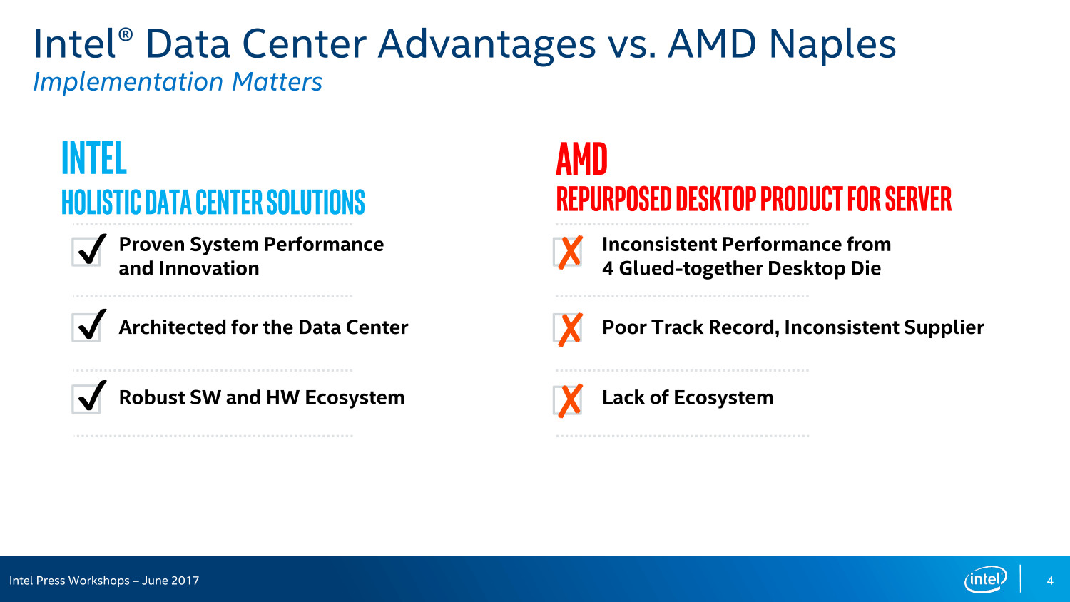
Intel’s glue is surely worse: can’t even allow Intel to stick to their marketing points against AMD.
I’m just going to sit here and enjoy Intel and AMD boxing like penguins. My opinion is that they’re trying to compete with each other on completly different fields so none of them will ever come out victorious in the end.
Now, now, Intel has holistic glue; that’s important difference.
Intel Holistic Enterprise-grade Glue™
for all your 22 nm to 14 nm, or 22 nm to 10 nm,
or 14 nm to 14 nm, or 14 nm to 10 nm,
or 10 nm to 10 nm needs.
Sounds very holistic to me. I wonder, will all this stickiness make it a worse box cutter for @wendell?
More seriously, what gets relegated to the 22 nm chunk? What is fine being slower than the I/O circuitry? Heat management? Something akin to POWER’s OCC?
I may be wrong on this but a bigger process does not strictly mean it will be slower, usually is is just that the larger it is the more heat it makes and thus has to be set slower to manage heat output. For these parts I do not think absolute max speed is a necessity so they can make them bigger and a little cheaper with better yields using an older well known process.
So may not be a drawback or compromise at all, just makes sense to them.
Well, in addition to heat reduction, you can pack the circuits more tightly together which I think would net you a speed increase due to the limited speed of electric fields through the silicon. I imagine that would let you do more per clock since, relative to the original design, a smaller process node increases the speed between components.
At 3 GHz light moves about 100 mm per clock. Electromagnetic waves in silicon would travel less than that, maybe 50 mm? I can’t guess specifics, but a smaller process node should mean less circuitry traversed per unit of time.