AMD Next Horizon - Livestream

The more I think about it the more I believe you and @denstieg are right here.

I am kind of torn on that one. On the one hand it makes sense for them to keep the segmentation of the product line. On the other hand memory and IO could be an easy way to one up Intel when it may become necessary.

yep, I agree

exactly! probably expensive though but a further advantage for the architecture

:thinking:

1 Like

You seem confused on the comment of the large victim cache. Let me put it into perspective.

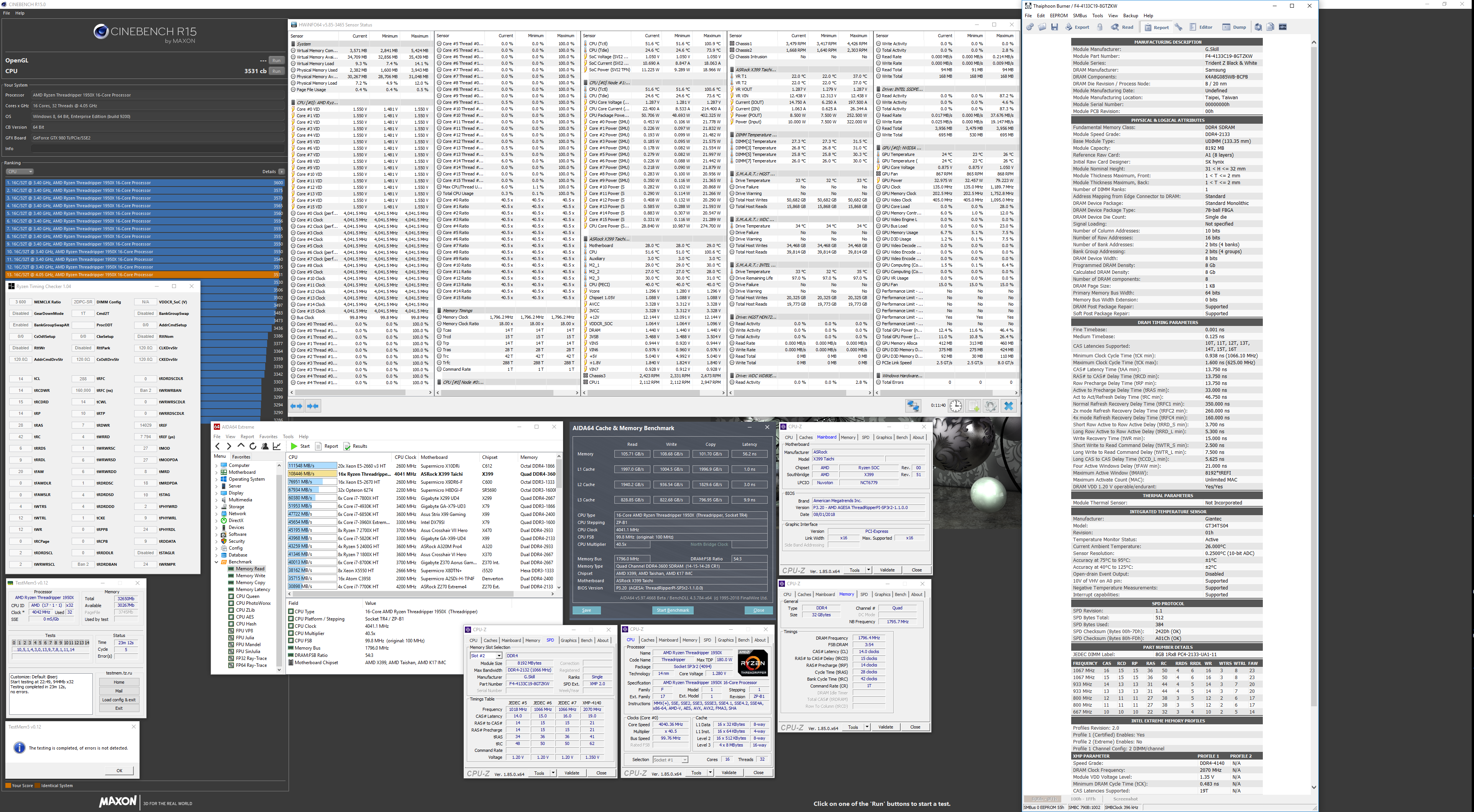
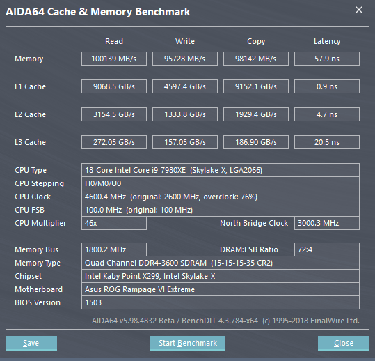
With AIDA64, measuring peak throughput, AMDā€™s L3 cache on TR is around 800GBps, while Intelā€™s L3 is around 200-300GBps. For overclocked ram on TR or Intel, you could see around 100GBps, and around 160GBps for Epyc.

So, AMDā€™s L3 has a peak around 3-4x that of Intelā€™s L3 cache speed, but the cache serves a different purpose: being a victim. That means it is a cache pool all cores will draw on and share, which means lots more calls, etc., so faster speeds help keep the data flowing as all cores can access it.

With the 32-core 2990WX, we saw that aside from the off die latency to get to the memory controller, there was more work keeping the cores fed using just 4-channel memory over the 8-channel Epyc chips.

So, what is the solution? Well, if you double the L3 cache per core to 4MB from 2MB, then double the cores with that, so long as you keep mem latency down and latency between dies and I/O chiplet down, then the faster L3 cache can serve up large amounts to the cores to keep them fed, combating the memory channel issues seen with the off-die access of the 2990WX. There is also the chance that speeds of the caches have been increased.

For example, the L2 caches between AMD and Intel solutions are roughly the same speeds, with slight edge on peak going to Intel. But, for L1 cache speeds, Intel is like double the speed of what is seen on AMD according to AIDA64, if not more. Some of that will be effected with AMDā€™s changes to the branch prediction, instruction pre-fetch, etc. So some other good changes to that were hinted at, while we will know more at launch, with some other hints coming before launch as well.

Does that make a little more sense on the larger cache size making up for not increasing the memory channels to a degree, which double the memory channels to double the memory bandwidth would still fall far short of the faster L3 cache speeds, and doubling the amount that can be held in that cache leaves it more on tap for the cores to call on.

1 Like


TR 1950X

image
7980XE

These are to show the cache differences between the two. The person with the 7980XE mentioned that before using the Beta, the L1 cache read at half of what is pictured here. The results in the first picture is my personal rig. Both performed in Windows 10 1803.

1 Like

Hmm have to find out/lookup the theoretical and practical difference and pro/cons to massive L3 or big L3 + L4 cash, that intel i7 5775c was a interesting chip for sure. 256mb of L3 is a little insane isnā€™t it?, I think 64mb L3 + 128mb of dram victim cash seem just a tad les of a insanity

image

WTF Rome isnā€™t out yet and now this?

OK its wwtalkoutarsTech but stil

I have not looked at it from that perspective yet. The only time I looked at performance impact of cache sizes and its bandwidth was with a very custom workload that had to move a lot of unique data. Maybe that is skewing my opinion on the benefit of large cache sizes. My workload probably was not very representative of other applications.

Is that what is meant with ā€œdepth of the frontendā€?

I think that makes more sense to me now. I would have to take a much closer look at CPU architectures to get a true understanding about all the dynamics here. My knowledge on this subject is very limited, but I am always excited about technology and interested in almost anything. Thatā€™s the reason I asked so many questions in this thread. :grinning:

Thanks a lot for the detailed post!

It depends on the purpose of the cache as to whether it makes sense. The purpose of cache is to keep data that is needed close in faster access memory chunks to prevent stalls waiting for calls from memory, generally. Cache fulfills that purpose. Granted, if look-up tables (LUTs) are too large, you then can defeat the purpose of having cache at all, so there is give and take. Meanwhile, 4MB isnā€™t out of the question AT ALL. If you kept the L3 at 2MB like for Zen and Zen+, that is 64MB for a 32 core chip and 128MB of L3 for a 64 core chip. What purpose, then, would an extra layer of L4 cache that is the same size as L3 serve, especially as usually L4 is slower than L3 is slower than L2 is slower than L1?

For example, when Intel used Crystal Well L4 cache, they gave 128MB of eDRAM to 4-cores as a victim cache, or 32MB per core. Here, we are talking L3, which is faster than eDRAM, and 4MB per core over 2MB. That doesnā€™t seem very unreasonable, especially looking at AMDā€™s speed on L3 versus Intelā€™s speed on L3. Here is an image looking at the latency implications of L4 cache on a Haswell chip which possessed that cache:

image


citing
https://www.anandtech.com/show/9320/intel-broadwell-review-i7-5775c-i5-5675c

You will notice that it kept the latency low until the cache was fully utilized, at which point it had to go off package to do the call from memory. This speeds up the ability for the cores to chew through the data until they have to wait the longer period for the data call from memory. Here is an article discussing the the On-Package I/O, when deployed with Crystal Well, would reach 102GB/s (far less than the 800GB/s I showed that I achieve with Zen 1 in my image above).

So I think you should take a step back and read those articles, spin the idea around for a little while, and maybe visit this wikipedia page on caches:

Ok so it was usefull as a speedup for igpu, like the HBM on the intel/amd coop, but for feeding the cores sorta pointles. Thanks for the info wil read it later, it just felt to massive 256mb for a old dude that comes from a time where casset tape and the realy big floppies where a thing. Hek i have more L3 on my 1700 than my first hard drive had space.

1 Like

This is why I also argue, even with the latency (which can be dealt with with the low latency HBM that has been developed for use with 3D chips in supercomputers), that HBM2 on package with 32GB having 1TB/s throughput in certain configurations (the speed, roughly, of AMDā€™s L3 cache) could speed up certain uses similar to how it was used with Xeon Phi accelerators. Considering we now are looking at 64 cores being fed, whereas the Xeon Phi Iā€™m referencing had like 50 cores at low speeds, it may be something to consider, with the DDR feeding the HBM on package. Then, the HBM would act like a massive L4 cache, while achieving over 100GBps per stack, much as the eDRAM accomplished, for the cumulative speed of the L3 cache speed around 800GBps. That way you have the 4TB+ of DDR feeding the 32GB of HBM of most called on items feeding the larger L3, etc.

But, that may not be viable until a package interposer is used rather than IF on MCM (please see the AdoredTV videos above and read through the cited whitepapers for AMD he references for use of interposers potentially in the future to reduce latencies, with this video discussing the financial costs of implementing an active interposer:


)

The fact that server chips now are reaching the number of cores a Xeon Phi had, but at faster frequencies, is really incredible as is, which also leads to looking at the mesh interposer Intel introduced with it around 2014, the use of HBM with the product despite people saying latencies are too high to use it for that, etc. In fact, if they put 16GB (4x4GB) of HBM2 or HBM3 on package with an interposer for mainstream chips or TR (although TR would do better with 32GB in 4x8GB stacks or 8x4GB with dual interposers for mem access) to give 512GBps-1TBps throughput, so long as latency was equal to roughly that of DDR, then it would truly act as a system on a chip and defeat the need for many users to have DDR (or, for workstations, free the DDR to be slower with more ranks similar to the upcoming 32GB DIMMs or quad rank LRDIMMs to focus more on ram capacity over speeds).

But those are just my musings on it, rather than specific speculation on planned products.

Edit: 64 core with a base of 2.35GHz.
https://reviewhardware.info/amd-64-core-rome-deployment-hlrs-hawk-at-2-35-ghz/

I calculated that number just by using 0.87 multiplied by the all core boost speed of the current 7601 chips which would give a 13% increase in IPC, which for double the performance meant lower speeds. Should have farmed that article out quicker before it was confirmed in a slide deck with HPE. Damn it!

A new one from the scottish one.